


 22 / 50

ADVANCED MATERIALS & PROCESSES •
OCTOBER 2014
22
ple structures to be sampled on a wafer. In a probe station
chamber, test structures can be tens of microns in size
(such as for the high-speed pHEMT device measurement
application described later in this article) or up to tens of
millimeters in size for measuring Hall structures.
Measuring devices in the vacuum chamber of a probe
station offer advantages as well. The variability in meas-
urements caused by humidity, condensation, and other en-
vironmental factors can be eliminated. Electronic
properties of some materials, such as organic semiconduc-
tors, can be significantly affected by surface contamina-
tion, and when measured under ambient conditions,
electrochemical leakage currents can obscure sensitive
current measurements. However, once the device is evac-
uated in a probe station, measurement conditions can be
restored. Additional options are available in cryogenic
probe stations for materials and devices where surface con-
tamination must be avoided. For example, high-vacuum
options are used to reduce the base pressure in the cham-
ber; in the advanced stations, the sample stage can be
maintained near room temperature during cool down of
the radiation shields so that residual gases are cryopumped
away from the sample space.
Also, when used in conjunction with sophisticated mo-
bility spectrum analysis software tools, vertical magnetic
field probe stations can be valuable for studying multilayer
or multi-carrier semiconductor Hall samples (such as mul-
tiply doped materials and heterostructures) by segregating
the mobility spectrum for each carrier species. By identi-
fying individual carriers, users can verify doping effective-
ness, correct for unwanted impurities during growth, and
control quality during various manufacturing stages.
Case study: Cryogenic probing
identifies off-state breakdown
Off-state breakdowns in
pseudomorphic high-electron-
mobility transistor
(pHEMT) devices result from the com-
plex interplay of material properties and device geometry.
Because gate-drain breakdown limits the maximum power
handling capability of these devices, this effect has been a
topic of interest since the inception of pHEMT device ar-
chitectures. Several physical mechanisms for the break-
down have been proposed and each has distinct
temperature dependencies that can be used to discern the
dominant mechanism in a given device architecture. Vari-
able temperature, on-wafer, transport measurements were
performed on a commercially available GaAs pHEMT
used in RF applications.
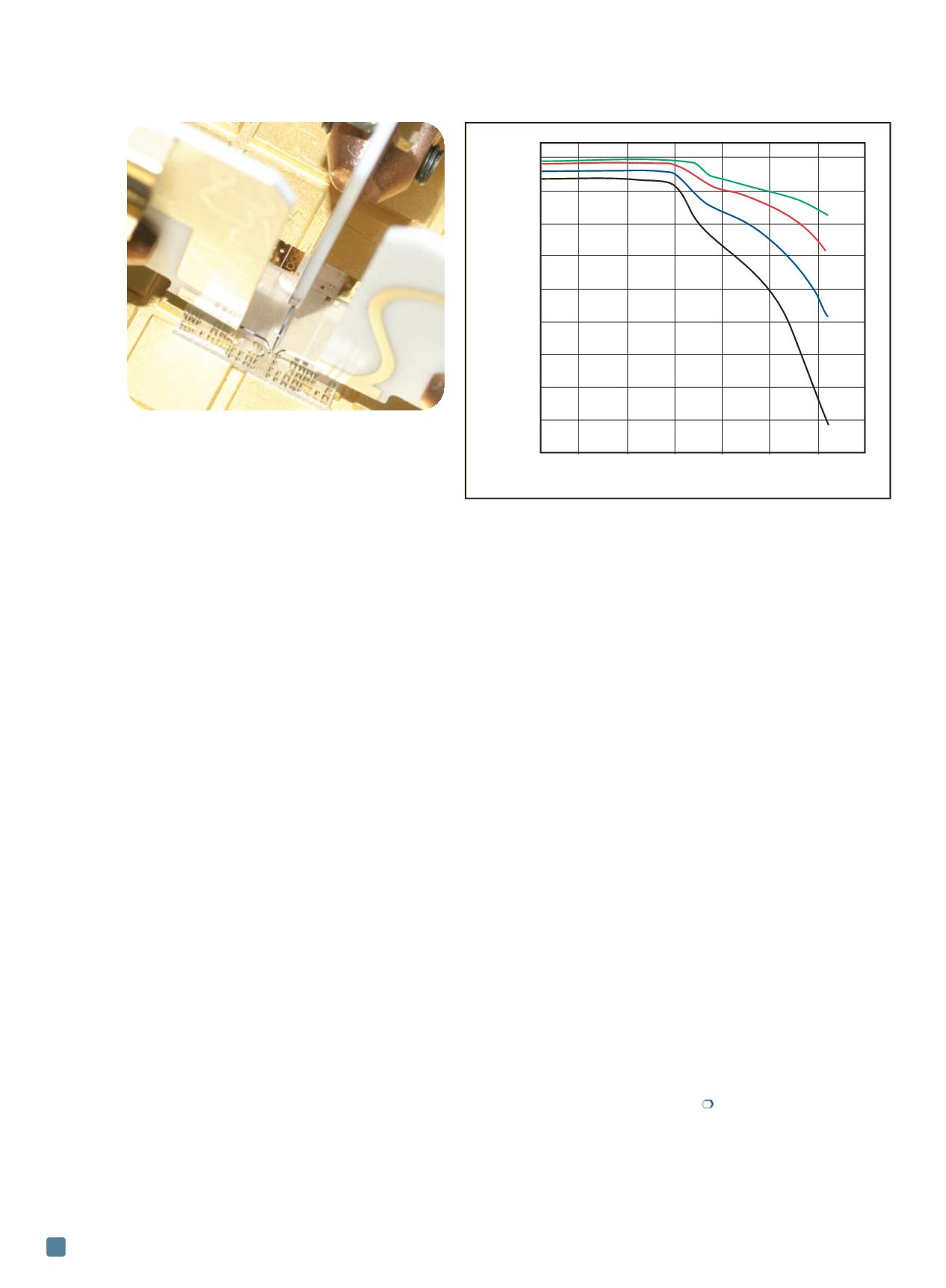
Three distinct gate leakage regimes are identified in the
temperature-dependent gate current for fixed source-gate
voltages in Fig. 3. Above 210 K, the nonmonotonic tem-
perature dependence of the gate current is indicative of a
thermionic field emission mechanism. Below 150 K, the
gate current is independent of temperature with a source-
gate voltage dependence, which suggests the barrier con-
duction is dominated by tunneling transport. Between 150
and 210 K, the observed temperature dependence of the
gate current indicates an intermediate breakdown mecha-
nism, perhaps defect-assisted tunneling.
Conclusion
Semiconductor research is becoming increasingly im-
portant to the development of higher-performing electron-
ics and computing technologies. Terahertz spectroscopy
bypasses the limitations of other characterization tech-
niques by enabling nondestructive measurement under
variable temperature and high magnetic field conditions. It
is in these environments that researchers can learn the
most about novel materials.
For more information:
Andy Phillips is marketing manager,
Lake Shore Cryotronics Inc., 575 McCorkle Blvd., Westerville,
OH 43082, 614.891.2243,
andy.phillips@lakeshore.com,
lakeshore.com.
Fig. 3
—
Three-terminal DC probing configuration for
transistor measurements.
Fig. 4
—
Temperature-dependent pHEMT gate current
during measurement of transfer curves (V
DS
= 3 V).
I Gate , A
V
GS
= -1.0 V
V
GS
= -1.5 V
V
GS
= -2.0 V
V
GS
= -2.5 V
50
100 150 200 250 300 350
Temperature, K
0.0
-20.On
-40.0n
-60.On
-80.On
-100.On
-120.On
-140.On
-160.On
-180.On