


 20 / 50

Andy Phillips
Lake Shore
Cryotronics Inc.
Westerville, Ohio
ADVANCED MATERIALS & PROCESSES •
OCTOBER 2014
20
W
ith the continuing demand for
higher computing performance, sig-
nificant research is being aimed at
characterizing novel materials for semiconduc-
tor use. Characterization of carriers as well as
unwanted impurities in materials will continue
to be an important step in the development of
next-generation semiconductor devices. Vari-
ous measurement techniques for Hall conduc-
tivity, carrier concentration, and mobility
measurements, as well as Raman and x-ray
spectroscopy, help to understand these materi-
als. However, many commercially available
technologies offer limited utility because they
do not account for material responses as a func-
tion of temperature, or their magnetic fields are
fixed, so it is impossible to differentiate mobil-
ities and carriers.
Many measurement platforms also do not
allow for noninvasive characterization of wafer-
scale materials or they require labor-intensive
bonding and packaging, making them imprac-
tical in current semiconductor materials test-
ing environments. New approaches to
nondestructive measurement for early stage,
temperature dependent materials characteriza-
tion under high magnetic field, as well as device
level, variable measurement testing will be ex-
plored, particularly as it relates to Hall analysis.
Temperature and early-stage
materials characterization
Analyzing at low temperatures is a common
method for isolating specific material phenom-
ena. Characterizing at variable temperatures
can also yield important insights into underly-
ing conductivity mechanisms. In particular, the
cryogenic environment reduces the inherent
noise of electronic materials, lessening its im-
pact on measurements. Certain carrier trans-
port properties are easier to detect at low
temperatures as well.
In some semiconductor materials, free car-
riers can be “frozen out” at cryogenic tempera-
tures while the intrinsic carrier concentration
or activation energy can be determined from
the temperature dependency of the carrier den-
sity. Knowing the material’s mobility and tem-
perature dependence can also help identify
concentrations of impurities and gauge poten-
tial saturation transconductance.
Continuous wave terahertz
For more than 20 years, researchers have
used terahertz frequency spectroscopy for ma-
terials characterization. The energy of terahertz
waves is low enough to couple to the free car-
rier motion in semiconductors. As a noncon-
tact, quasi-optical technique, terahertz
spectroscopy is ideal for characterizing the con-
ductivity of bulk semiconductors, ultrathin epi-
layers, and buried thin films in pre-device stage
heterostructures.
Terahertz spectroscopy at cryogenic tem-
peratures can expose properties not apparent
at room temperature and allows carrier con-
centration and semiconductor mobility to be
tuned. However, most commercially available
THz systems lack the necessary cryogenic and
magnetic environments required for targeted
semiconductor materials research, and if they
do have them, THz energy is usually generated
outside the testing environment. With these
optical cryostat-based systems, THz beams
must pass through windows—reducing signal
power and causing spectral distortion—and
their optics are difficult to align, which can lead
to repeatability issues.
However, all of this is changing with im-
provements in how THz energy is generated
and applied to materials under test. Newer
con-
Nondestructive Variable Temperature
Materials Characterization
for Semiconductor Research
To meet the
rigorous
demands of
next-generation
computer
technology, new
approaches to
nondestructive
measurement
for early stage,
temperature
dependent
materials
characterization
are needed.
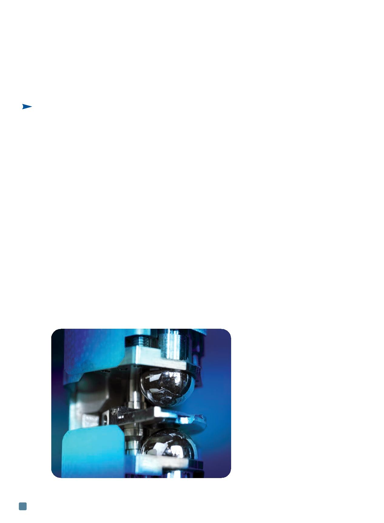
Continuous wave-THz spectroscopy system emitter and detector devices
for semiconductor materials characterization.