


 16 / 50

news
industry
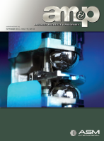
Shrinking plastic closes nanowire gap
Engineers at the University of Illinois at Ur-
bana-Champaign are using Shrinky Dinks—plastic
that shrinks under high heat—to close the gap be-
tween nano-wires in an array to make them useful
for high-performance electronics applications.
Nanowires are placed on the Shrinky Dinks plastic
just like any other substrate, and then shrunk to
bring the wires much closer together. This enables
creation of very dense arrays of nano-wires in a
simple, flexible, and controllable process. The new
method also brings the nanowires into alignment
as they increase in density. Wires even more than
30° off-kilter can be brought into perfect alignment
with their neighbors after shrinking.
For more information: SungWoo Nam, 217.300.0267,
swnam@illinois.edu,
illinois.edu.
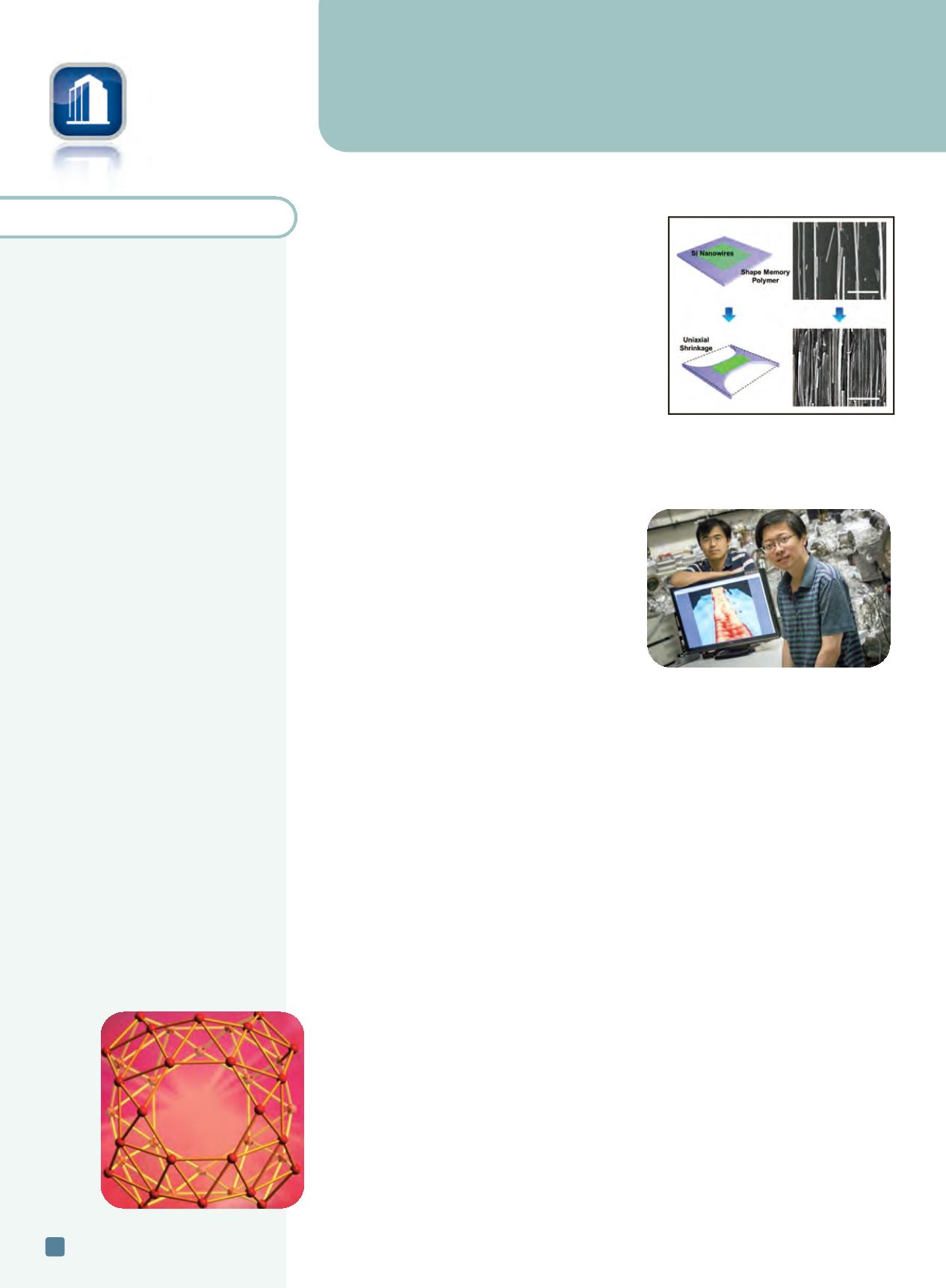
Graphene ribbons: Size matters
Using graphene ribbons of unimaginably
small widths—just several atoms across—a
group of researchers at the University of Wis-
consin-Milwaukee (UWM) found a novel way
to “tune” the wonder material, causing the ex-
tremely efficient conductor of electricity to act
as a semiconductor. In principle, their method
for producing these narrow ribbons and manip-
ulating the ribbons’ electrical conductivity
could be used to produce nanodevices.
“Nano-ribbons are model systems for studying nanoscale effects in graphene, but obtain-
ing a ribbon width below 10 nm and characterizing its electronic state is quite challenging,”
says postdoctoral researcher, Yaoyi Li. By imaging the ribbons with scanning tunneling mi-
croscopy, researchers confirmed hownarrow the ribbonwidthmust be to alter graphene’s elec-
trical properties, making it more tunable.
“We found the transition happens at three nanometers and the changes are abrupt,”
says Lian Li.
For more information: Lian Li, 414.229.5108,
lianli@uwm.edu,
uwm.edu.
Mythical boron buckyball does exist
Researchers from Brown University, Providence, R.I., as well as Shanxi University and
Tsinghua University, China, have shown that a cluster of 40 boron atoms forms a hollowmo-
lecular cage similar to a carbon buckyball. It is said to be the first experimental evidence that
a boron cage structure—previously only a matter of speculation—does indeed exist.
Chemistry professor Lai-Sheng Wang and his research group showed earlier this year
that clusters of 36 boron atoms form one-atom-thick disks, which might be stitched to-
gether to form an analog to graphene, dubbed borospherene. Boron clusters with 40 atoms
are also abnormally stable compared to other boron clusters. Figuring out what that 40-
atom cluster actually looks like required a combination of experimental work and model-
ing using high-powered supercomputers.The borospherene molecule is not quite as
spherical as its carbon cousin. Rather than a series of five- and six-membered rings formed
by carbon, borospherene consists of 48 triangles, four seven-sided rings, and two six-mem-
bered rings. Several atoms stick out, making the surface of borospherene somewhat less
smooth than a buckyball.
For more information: Lai-Sheng Wang, 401.863.3389,
lai-sheng_wang@brown.edu,
brown.edu.
Researchers show that clusters of 40 boron atoms form a molecular cage similar to
the carbon buckyball. Courtesy of Wang lab/Brown University.
ADVANCED MATERIALS & PROCESSES •
OCTOBER 2014
16
N
ANOTECHNOLOGY
briefs
Scientists at
AMBER,
a materials
science center based at
Trinity
College Dublin,
Ireland,
discovered a new material that
could revolutionize information
technology, computer processes,
and data storage. The research
group led by Michael Coey created
a new alloy of manganese,
ruthenium, and gallium, known as
MRG. The alloy is a strange new
magnet—internally it is as
magnetic as the strongest magnets
available, but from the outside it
does not appear magnetic. The
material (technically known as a
zero-moment half metal)
will
initiate a completely new line of
materials research and could open
up numerous possibilities for
electronics and information
technology.
www.tcd.ie.
Applied Materials Inc.,
Santa
Clara, Calif., announced two new
systems to help solve critical
challenges in manufacturing high-
performance, power-efficient 3D
devices. The Applied Reflexion LK
Prime CMP system provides
superior wafer polishing
performance with nanometer-level
precision for FinFET and 3D NAND
applications. The Applied Producer
XP Precision CVD system solves
demanding, fundamental
deposition challenges presented by
vertical 3D NAND architectures.
These new CMP (chemical
mechanical planarization) and CVD
(chemical vapor deposition) tools
directly address precision,
materials, and defect issues,
enabling 3D designs to reach high-
volume manufacturing.
appliedmaterials.com.
Plastic is clamped so it only shrinks in one
direction. Courtesy of SungWoo Nam.
Yaoyi Li (foreground) and Mingxing Chen
display an image of a ribbon of graphene
1 nm wide. Atoms are visible as bumps.