


 1 / 58

edfas.org
1
ELECTRONIC DEVICE FAILURE ANALYSIS | VOLUME 19 NO. 2
DEPARTMENTS
56 ADVERTISERS’ INDEX
Positron Beams as E ective Nondestructive Analysis Tools for the Semiconductor IndustryManfred Fink, Jeremy Johnson, and S.V. Nguyen
Positron spectroscopies offer aunique level of precision for
defect detection and identification. The development of
the deflection focusingpositrongun increases the intensity
of a traditional positronbeam, making it amore useful tool
for the semiconductor industry.
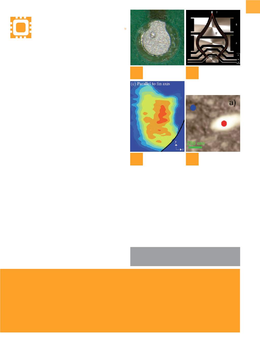
ABOUT THE COVER
Scanning electron microscopy photo showing lifted-out tin
dendrite that caused a flip-chippin-to-pin short. The dendrite
was sitting between ball grid array balls in a flip-chip package
where the energy-dispersive spectroscopy (EDS) signal was
blocked. The dendrite was lifted out with an Omniprobe and
put on carbon tape for EDS analysis.
Photo by Nathan Wang,
Maxim Integrated, First Place Winner in Black &White Images,
2016 EDFAS Photo Contest.
Author Guidelines
Author guidelines and a sample article are available at edfas.
org. Potential authors should consult the guidelines for useful
information prior to manuscript preparation.
4 10A RESOURCE FOR TECHNICAL INFORMATION AND INDUSTRY
DEVELOPMENTS
MAY 2017
|
VOLUME 19
|
ISSUE 2
edfas.org
ELECTRONIC DEVICE
FAILURE ANALYSIS
54 DIRECTORY OF FA PROVIDERS
Rose Ring
49 EDFAS AWARDS Cheryl Hartfield
55 GUEST COLUMNISTDavid Burgess
2 GUEST EDITORIAL Larry Wagner
35 INTERNET RESOURCES
Rose Ring
42 INVENTOR'S CORNER
Jim Colvin
52 LITERATURE REVIEWMike Bruce
44 PRODUCT NEWS Larry Wagner
48 TRAINING CALENDAR
Rose Ring
40 UNIVERSITY HIGHLIGHT
Mike Bruce
38 2017 PHOTO CONTEST
39 2017 VIDEO CONTEST
Advantages and Challenges of 3-D Atom Probe Tomography Characterization of FinFETsAndrew J. Martin, Ajay Kumar Kambham, and Ahmad D.
Katnani
A case study highlights the use of atomprobe tomography
for failure analysis of next-generation technologies.
22For the digital edition, log in to edfas.org,
click on the "News/Magazines" tab, and
select "EDFA Magazine."
Failure Analysis on Soldered Ball Grid Arrays: Part IIGert Vogel
This article continues the analysis of voids in BGA balls
and includes case studies with plane parallel polishing of
a printed circuit board assembly.
Characterizing Organic Nano- contamination in Semiconductors by Resonance-Enhanced Nanoscale IRSpectroscopy (AFM-IR)
Anirban Roy and Jay Anderson
Read about resonance-enhanced AFM-IR, an emerging
technique with the potential to overcome the limitations
of existing tools in semiconductor fabs and failure analysis
labs.
31 10 22 31 4