


 8 / 58

edfas.org
ELECTRONIC DEVICE FAILURE ANALYSIS | VOLUME 19 NO. 2
8
like a silvery disk in the microscope when viewed from
the backside. Copper deposition after the desmearing
process is not always able to close the hole in the copper
layer (Fig. 14). This means that some moisture from the
PCB resin evaporates into the liquid solder ball during the
reflow soldering process, which results in large voids that
are identified during x-ray inspection. The supplier of the
PCB confirmed that the laser had been replaced without
subsequently calibrating the energy level.
SUMMARY
Based onmany case studies, it was shown that failure
analysis on soldered BGAs encompasses a wide range of
possible failure mechanisms. Failures can originate in
manymanufacturing process steps. The stencil printing of
the solder paste is often a critical process, but more often,
faulty PCBs represent the root cause. However, defective
silicon in the BGAs is extremely rare.
Making cross sections of soldered BGAs is a common
approach when analyzing failures. Two new approaches
were presented as additional methods for identifying
the root causes of failures. Grinding away the corpus of
the BGA while the soldered balls are still left on the PCB
can provide insight into the failure mechanism. On the
other hand, confirmation that all solder connections are
perfect can indicate that there is a fault in the PCB layout.
Grinding away the complete PCB from the backside until
the base of the soldered balls can be viewed allows an
electronic pathologist to check the quality and alignment
of the microvias.
The combination of thesemethods with expert knowl-
edge of all the various steps in the fabrication of PCBs
and PCBAs can solve many problems in the production
of electronic assemblies.
Fig. 11
Cross section showing voids in the soldered BGA balls, but no misalignment is evident
Fig. 12
Grinding away the complete PCBA under the
microvias shows that the inner copper layer hadbeen
perforated while lasering the microvias.
Fig. 13
Perforated copper pads of thefirst inner layer viewed
from below
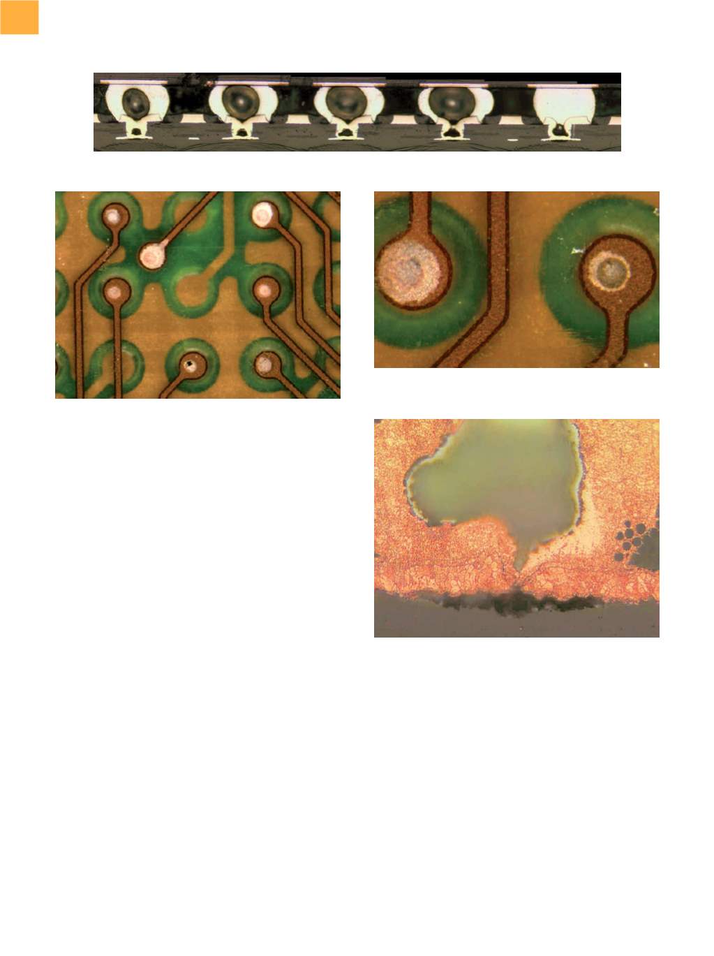
Fig. 14
Cross section of a perforated copper pad. Chemical
desmearing of the microvia after lasering dissolved
some of the PCB resin beneath the copper pad. Under
the microscope, this void looks like a silvery disk
when viewed from below.
FAILURE ANALYSIS ON SOLDERED BALL GRID ARRAYS: PART II
(continued from page 6)