



 13 / 58

edfas.org
13
ELECTRONIC DEVICE FAILURE ANALYSIS | VOLUME 19 NO. 2
in industry. One significant source of limitation is the inef-
ficiency in the moderation process; the other lies in the
sources commercially available. The deflection focusing
positron gun (DFPG) developed at The University of Texas
addresses both of these limitations.
The DFPG has been designed to generate the most
intense source-based slow positron beams. Positrons
are created in a large ring of radioactive material. This
source geometry dramatically increases the number of
positrons generated by simply increasing the surface area
of the source that is contributing positrons to the beam.
Secondly, the DFPG uses advances in moderator geom-
etries to more efficiently produce moderated positrons.
The geometry of the DFPG also suppresses background
counts by greatly reducing the number of unmoderated
positrons leaving the gun.
POSITRON INTERACTIONS IN MATTER
Positrons are the antimatter partner of the electron.
The two particles have the same mass, but the positron
has an opposite charge. When slowpositrons—thosewith
less than a fewmegaelectron volts—encounter ametal or
semiconductor, three categories of outcomes are possible:
reflection, absorption and re-emission, and annihilation,
as depicted in Fig. 2.
A fraction of the positrons in a beamwill be scattered
elasticallywhen they encounter a surface. More positrons
are diffracted in this way when the beam energy is lower.
Measurement techniques such as low-energy positron
diffraction can use these diffracted positrons to develop
an interference pattern, which relays information about
the arrangement of the atoms at the surface of a metal or
semiconductor.
[6]
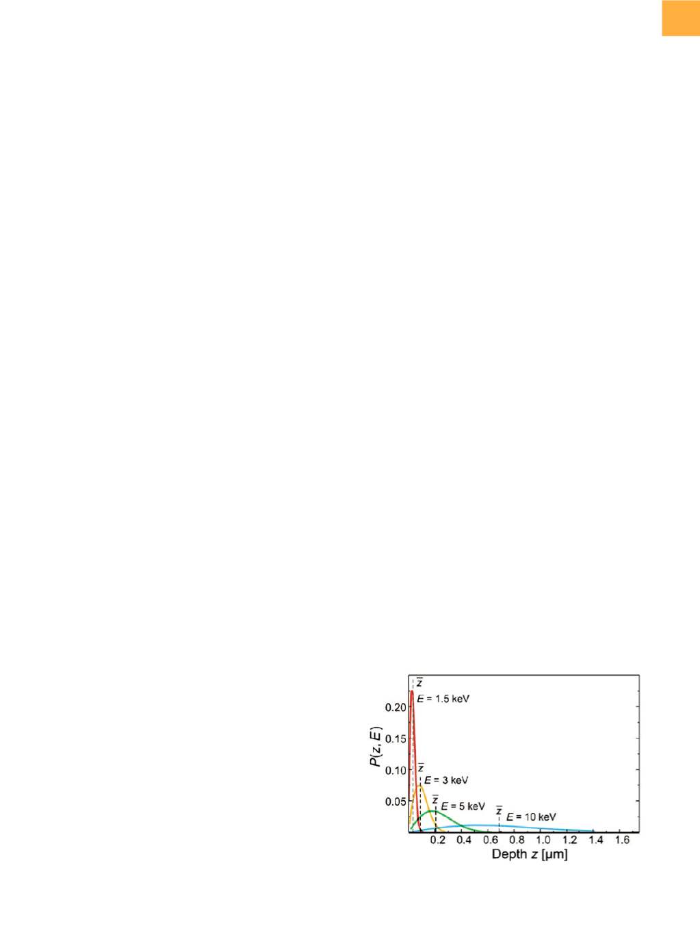
Positrons penetrate to an average depth that increases
with their initial kinetic energy. During this process, the
positrons undergo repeated inelastic deflections, losing
energy primarily through the creation of phonons and
plasmons. The implantation depths for a given positron
kinetic energy have a Makhovian profile.
[7]
An example
of implantation profiles for varying energies is shown in
Fig. 3.
Positrons lose energy via inelastic collisions until they
have thermalized with the material. Some may arrive at
a surface before they have fully thermalized; otherwise,
they diffuse through thematerial with an energy of
kT
until
they annihilate with an electron or arrive at a surface.
Anumber of things canhappenwhenapositronarrives
at the surface. If the surface has a positive work function
greater than the positron’s energy, the positron may
become trapped there. If the positron has enough energy
to escape, it may be emitted as an epithermal positron,
or it may pick up an electron from the surface and escape
as neutral, atomlike positronium. If the positronic work
function
f
+
is negative, a thermalized positron may be
emittedwithan energy of
kT
+
f
+
, allowing for the creation
of monoenergetic positron beams.
Positrons that do not end up back at the surface are
annihilated in the interior of the sample. Positrons in a
material have a diffusion length that is determined by the
material itself and its configuration. In a perfect crystal
lattice, this length is usually approximately 150 nm. Lattice
defects with regions of high local negative charge, such
as dislocations, vacancies, and near-certain impurities,
can trap positrons. In this case, their diffusion length is
diminished, but their lifetime is extended. Different types
of defects are associatedwith distinct lifetimes, which can
even be used to distinguish between different arrange-
ments of the same type of defect. For example, one can
determine if dopants tend to exist as single atoms, inpairs,
or in larger clusters, and in what ratios.
Positrons remaining in a sample eventually find an
electron and are annihilated. There are a number of
channels for this reaction to proceed down, but 99.7% of
the reactions result in the emission of two photons back-
to-back in the frame of the interaction. Each photon has
an energy very close to the mass energy of the electron
or positron: 511 keV. Because the electrons in the sample
are moving, there may be a difference between the refer-
ence frame of the interaction and that of the lab frame of
several electron volts. Tightly bound core-shell electrons
move much faster than outer-shell or conduction band
electrons and therefore showa greater difference fromthe
lab frame. This appears either as an increasing opening
angle when the moment difference is more transverse
to the direction of flight of the photons or as a greater
Fig. 3
Makhovian implantation profiles in single-crystal
silicon. Source: Ref 8