



 12 / 58

edfas.org
ELECTRONIC DEVICE FAILURE ANALYSIS | VOLUME 19 NO. 2
12
encounters an electron, they annihilate. Approximately
99.7% of such collisions result in the emission of two
511 keV (kiloelectron volts) photons back-to-back in the
frame of reference of that collision.
[1]
Deviation from lin-
earity of thephotons in the laboratory frame arises primar-
ily from the momentum of the electron, and this was first
used tomeasure the Fermi surfaces of metals and alloys.
[2]
The difference in charge of the positron from that of
the electron creates a number of important differences
in its interactions with matter. Positrons tend to become
trapped in regions of high electronegativity, such as in
dislocations, vacancies, or around some types of impuri-
ties in the sample. Additionally, the photoelectric work
function can be negative for surfaces of some materials.
For electrons, a material’s work function (
f
−
) is always
positive; energy must be put into the electrons to free
themfromthe surface. For positrons, however, the surface
dipole potential (
D
) in the work function has the opposite
sign of the bulk chemical potential (µ), and so the positron
work function (
f
+
) is very nearly zero andmay be negative
according to:
[3]
f
−
= +
D
– µ
−
f
+
=
−
D
− µ
+
If a positron inside the bulk of the material reaches
such a surface, it will be ejected from the sample, picking
up the work function energy. This is the mechanism
behind positron moderation, which allows the creation
of monoenergetic positron beams. Unfortunately, it is a
highly inefficient process.
Positrons penetrate a sample to an average depth that
depends on their energy. A beam of a few electron volts
samples only the first monolayer of the sample, whereas
a positron in a beamof 35 keV can penetrate to a depth of
10 µm. This allows for depth-dependent characterization
of defects in a sample.
[4]
Positrons in slowpositron beams originate fromeither
pair production or radioactive decay. Pair production
techniques require either an accelerator, such as the Elbe
PositronSource inDresden, Germany, or a nuclear reactor,
such as the Neutron-Induced Positron Source at Munich
(NEPOMUC). These systems allow for the creation of
positron beams of incredible intensity (3
×
10
9
moderated
positrons per second in the case of NEPOMUC), limited
only by the count rate of the detectors or, in some cases,
the capability of components of the beam to dissipate
heat.
[5]
Unfortunately, all of these systems also require
large facilities and thus must compete for resources
with other projects and suffer the facilities’ downtimes.
This makes them expensive and unsuitable for extensive
industrial use. Traditional source-based positron beams
are relatively inexpensive to build and operate and can
be constructed anywhere, because they only use a por-
table radioactive sample. However, they are limited by
low positron count rates, and that translates to longer
measurement times, which has limited their application
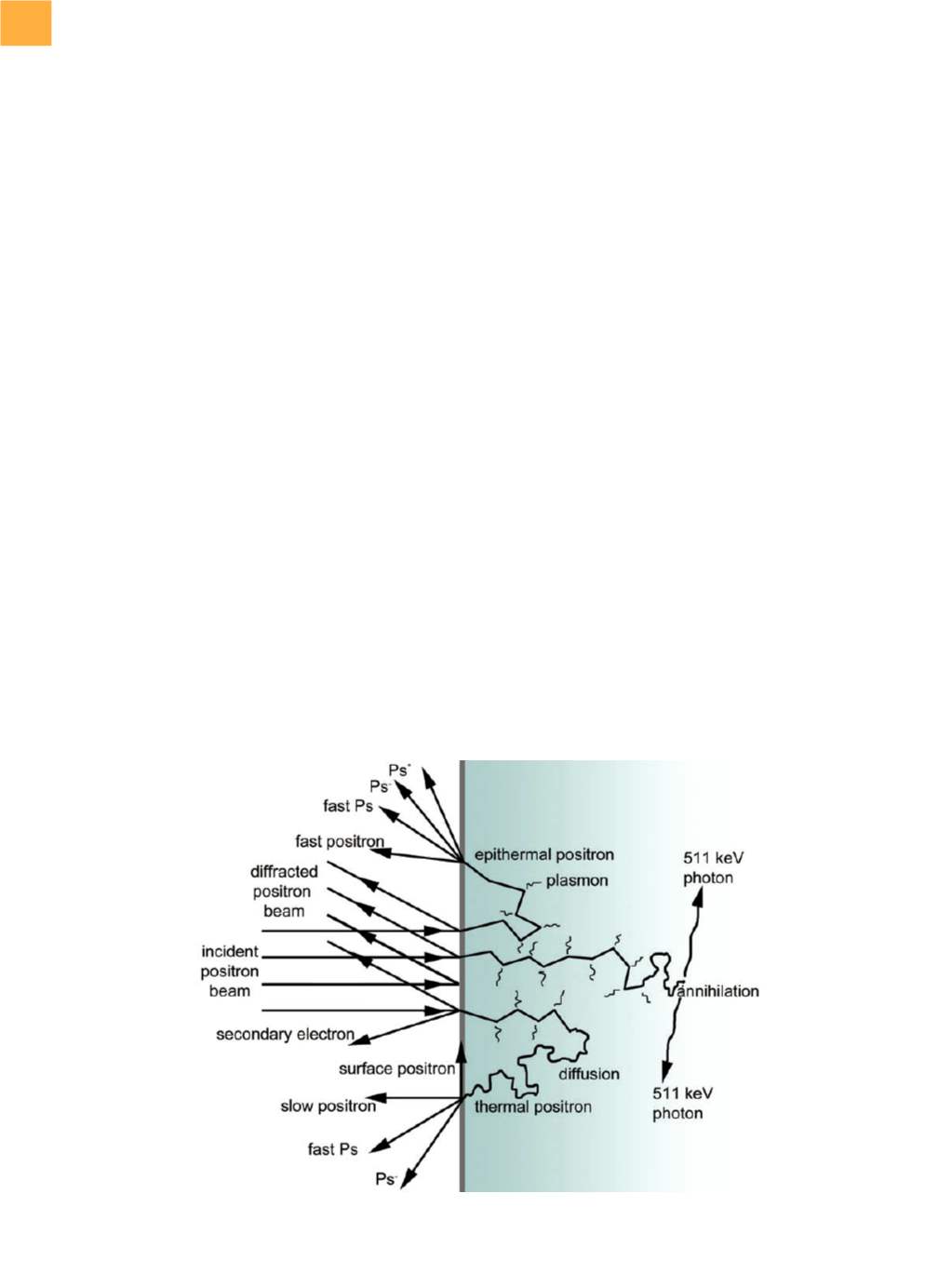
Fig. 2
The multitude of possible interactions between a positron (Ps) beam and a metal or semiconductor target
POSITRON BEAMS AS EFFECTIVE NONDESTRUCTIVE ANALYSIS TOOLS
(continued from page 10)