


 10 / 58

edfas.org
ELECTRONIC DEVICE FAILURE ANALYSIS | VOLUME 19 NO. 2
10
POSITRON BEAMS AS EFFECTIVE
NONDESTRUCTIVE ANALYSIS TOOLS FOR THE
SEMICONDUCTOR INDUSTRY
Manfred Fink, Jeremy Johnson, and S.V. Nguyen
Physics Department, The University of Texas
fink@physics.utexas.edu jjohnson@physics.utexas.eduINTRODUCTION
Slow positron beam spectroscopies are capable of
revealing information about the arrangement of dopants
and defects in a metal or semiconductor sample with a
resolutionbetter than a single atomic lattice site at depths
typically up to a few micrometers. Information on this
scale at depths more than a few monolayers cannot be
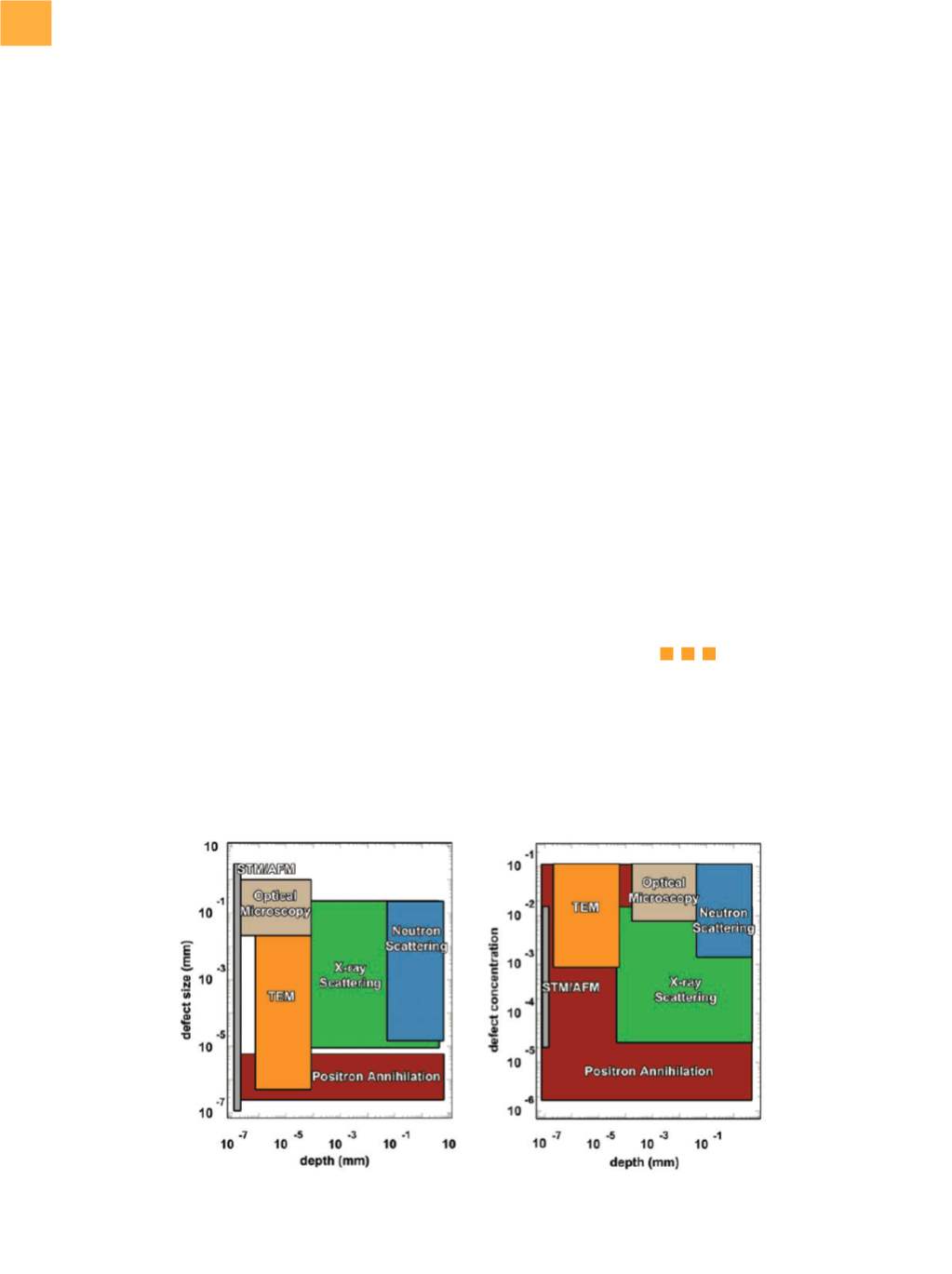
achieved by any other spectroscopic technique. Figure
1 shows a comparison of techniques. Furthermore,
the sensitivity range for open-volume defects starts at
approximately one vacancy per 10
7
atoms. This enormous
sensitivity comes about because a thermal positron can
diffuse approximately 100 nm in the bulk of a material,
and so each can probe a large number of lattice sites.
Furthermore, positrons annihilate with only the easily
EDFAAO (2017) 2:10-20
1537-0755/$19.00 ©ASM International
®
replaced electrons, making positron spectroscopies
nondestructive. The slow positron beam is a uniquely
useful tool when it comes to characterizing and evaluat-
ing semiconductors.
The positron is the antimatter partner of the electron;
it is identical but with a positive charge. When a positron
“POSITRONS TEND TO BECOME
TRAPPED IN REGIONS OF HIGH
ELECTRONEGATIVITY, SUCH AS IN
DISLOCATIONS, VACANCIES, OR
AROUND SOME TYPES OF IMPURITIES
IN THE SAMPLE.”
Fig. 1
Comparison of the capabilities of spectroscopic techniques. Positrons are capable of discerning defects smaller than an
atom and can penetrate deeply into a sample.
(continued on page 12)