


 6 / 58

edfas.org
ELECTRONIC DEVICE FAILURE ANALYSIS | VOLUME 19 NO. 2
6
standard cross section. The backside of the PCBA in the
BGA area is polished down to just under the first inner
layer of the PCB. Plane parallel polishing of several square
centimeters of a PCB to an accuracy of ±10 µm in depth is
assisted by the layered structure of the PCB. Grinding is
stopped approximately 50 µm below the interesting first
inner layer, and the plane is polished. Using polarized
light, one can look through the rest of the resin and the
glass fibers of the PCB (Fig. 7). In this case study, the inner
layer is misaligned. All the microvias are open to the bulk
of the PCB. In the cross section of Fig. 3, themisalignment
is in the plane of the cross section. Figure 8 shows the
more common situation: a misalignment under an angle
of 45°. The image clearly shows that cross sections through
such a copper pad under 90° or 180° would not provide
indisputable evidence.
This is also valid for the “blowout” failure mode. In
most cases, the holes in the copper sleeve of a through-
hole are located at angles of 45° and therefore are hard
to find with a cross section. If a section of a PCB with
blowouts is heated in glycol to >100 °C, bubbles can be
seen escaping from the through-holes. They primarily
originate at an angle of 45° (Fig. 9). This is not by chance
but depends on the alignment of the woven glass fibers
in the PCB.
A misalignment of the microvias is not always the
reason for an increased incidence of large voids in BGA
solder joints. The next case study once again shows a row
of big voids under x-ray inspection (Fig. 10). A cross section
shows the voids, but no misalignment of microvias could
be detected (Fig. 11). As before, the PCBwas ground down
underneath themicrovias, and the bottomside of the first
inner layer was viewed using polarized light (Fig. 12). This
revealed that the inner copper layer had been perforated
when lasering the microvias (Fig. 13). This information
explains the appearance of the cross section of a perfo-
rated copper pad. Chemical desmearing of the microvia
after lasering dissolved some of the PCB resin beneath the
copper pad. After parallel cross sectioning, this gap looks
(continued on page 8)
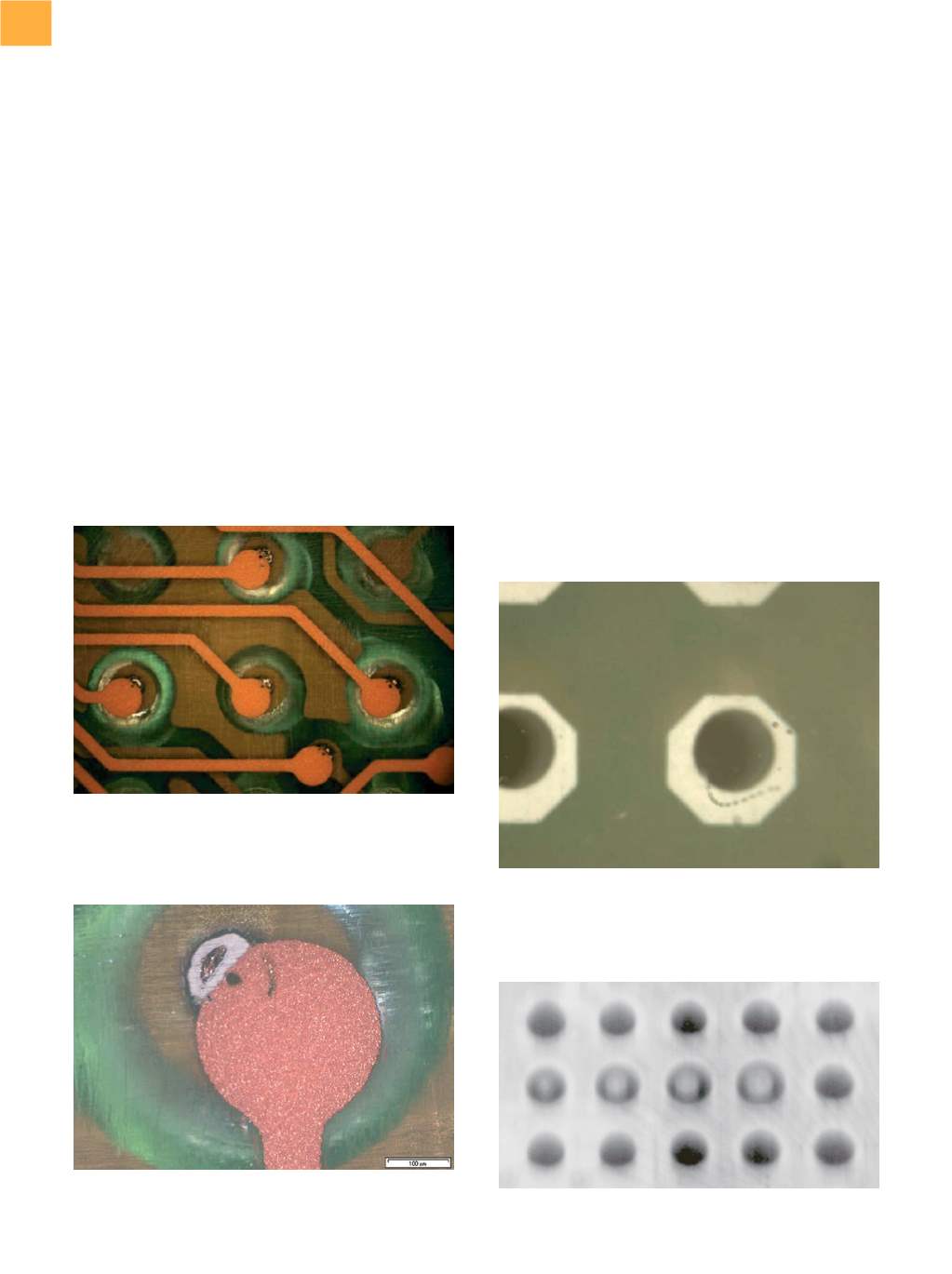
Fig. 7
Plane parallel grinding of the PCBA fromthe backside
to 50 µm below the first inner layer. The inner layer
is misaligned. All microvias are open to the resin of
the PCB.
Fig. 8
Magnified view of Fig. 7 showing detail of the
misalignment
Fig. 9
PCB with “blowout” failure pattern. Bubbles
come out of a through-hole when heated in glycol.
The location of the hole in the copper sleeve lies
predominantly below 45° to the PCB alignment.
Fig. 10
X-ray image of large voids in soldered BGA balls