


 5 / 58

edfas.org
5
ELECTRONIC DEVICE FAILURE ANALYSIS | VOLUME 19 NO. 2
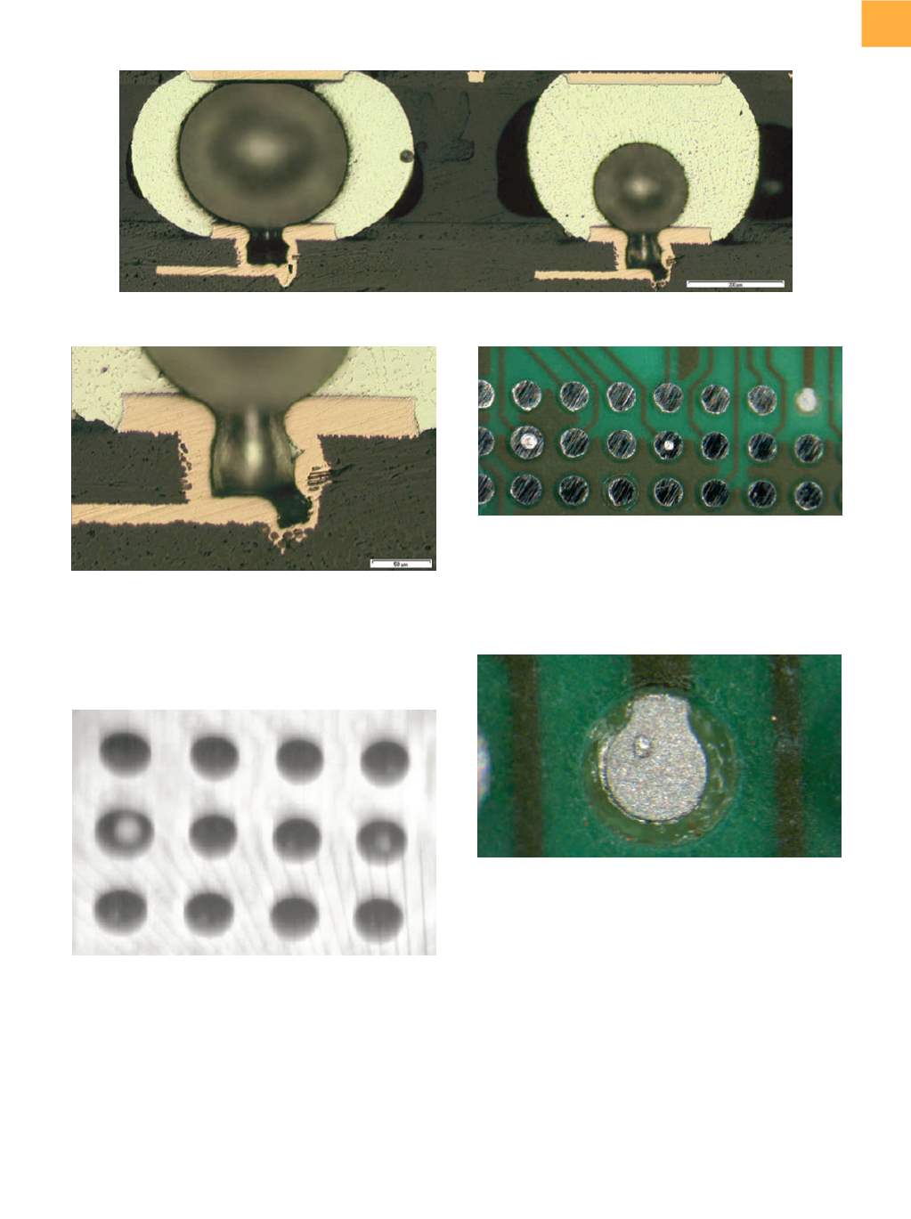
large void, but also an unobtrusive ball had dropped off
the solder pad (Fig. 5). The root cause of the failure was
now clear: A clogged stencil was again responsible, this
time combined with a particle of the dried flux in the
printed solder paste. The ball that had dropped off pro-
vided the indisputable evidence (Fig. 6). Performing only
a cross section parallel or perpendicular to the BGAwould
not have provided sufficient evidence to indicate that a
clogged stencil was the problem.
PLANE PARALLEL POLISHING DOWN OF
A PCBA
If large voids are seen during x-ray analysis and there
is suspicion that problems with microvias could be the
reason for these voids, an alternative analysis method
developed for this purpose is applied instead of the
Fig. 2
Cross section showing the failure: maladjustment of the microvias between the outer and the first inner layer
Fig. 3
Cross section showing the root cause of the failure:
misalignment between the microvia and the copper
land of the first inner layer. The microvias are open
to the resin of the PCB. Evaporating moisture from
the PCB inflates the molten solder during reflow
soldering.
Fig. 4
Another BGA after reflow soldering. X-ray analysis
shows two voids.
Fig. 5
Plane parallel grinding of the BGA to the center of
the voids. The large void on the left has an angular
particle in it. This is dried flux from the solder paste
that came off a stencil that had not been thoroughly
cleaned. Surprisingly, one unobtrusive ball on the
upper right dropped out.
Fig. 6
The footprint of thedropped-out ball shows that there
was a problem with a clogged stencil mask while
printing the solder paste. Just one small solder bead
was transferred to the pad.