


 4 / 58

edfas.org
ELECTRONIC DEVICE FAILURE ANALYSIS | VOLUME 19 NO. 2
4
EDFAAO (2017) 2:4-9
1537-0755/$19.00 ©ASM International
®
FAILURE ANALYSIS ON SOLDERED BALL GRID ARRAYS:
PART II
Gert Vogel, Siemens AG, Digital Factory Division, Control Products, DF CP QM SQA 5
gert.vogel@siemens.comINTRODUCTION
In the February 2017 issueof
EDFA
magazine, the failure
analyis of soldered ball grid arrays (BGAs) with plane
parallel removal of the BGA was discussed. In this second
part, the analysis of voids in the BGA balls is continued,
including case studies with plane parallel polishing of a
printed circuit board assembly (PCBA).
TYPICAL ERROR PATTERN: LARGE
VOIDS IN THE SOLDERED BGA BALLS
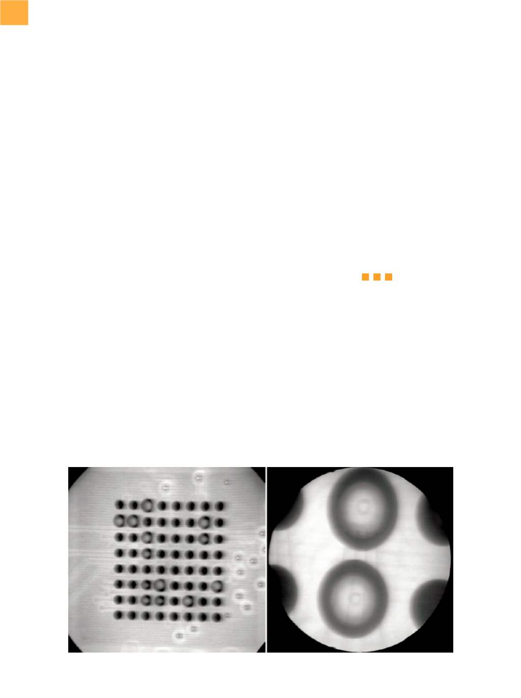
Large voids in BGA solder joints covering more than
30% of the ball area in the x-ray image (Fig. 1) are con-
sidered to be failures, in accordance with IPC-A-610,
“Acceptability of Electronic Assemblies,” and they result
in the PCBA being rejected.
If the failure analysis shows indisputably that the
failure was caused by a misalignment of the first inner
layer, then it is possible tomakea claimagainst theprinted
cirucit board (PCB) supplier. In our example, a metallo-
graphic cross section (Fig. 2, 3) was used to demonstrate
this misalignment.
It is not always possible to clearly identify the root
cause, as in the above example. A cross section frequently
shows only the voids but provides no evidence of the
specific cause.
Sometimes, the previously mentioned preparation
by polishing down the BGA allows the root cause to be
determined, as shown in the next case study. Here, two
eye-catching voids were seen during x-ray inspection (Fig.
4). For analysis, the specimen was first ground down to
the center of the voids. This subsequently provided a cross
section in the vertical axis for further analysis. Surprisingly,
not only was a sharp-edged organic particle found in the
“BASED ON MANY CASE STUDIES, IT WAS
SHOWN THAT FAILURE ANALYSIS ON
SOLDERED BGAs ENCOMPASSES A WIDE
FIELD. FAILURES CAN ORIGINATE IN MANY
MANUFACTURING PROCESS STEPS.”
Fig. 1
X-ray of a BGA with many large voids. The microvias can be seen at the center of the voids.