


 25 / 66

edfas.org
25
ELECTRONIC DEVICE FAILURE ANALYSIS | VOLUME 18 NO. 4
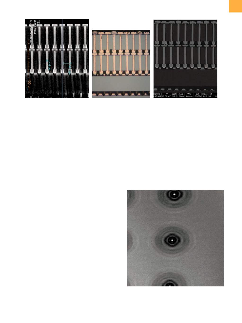
(a)
(b)
resolution, but there are promising developments for
both techniques. Recent advances in 3-D x-raymicroscopy
(XRM)/tomography demonstrate a submicron resolu-
tion of 0.7 µm, even down to 50 nm for special systems.
However, this extreme resolution requires relatively small
samples and/or a very long measurement time (several
hours). Provided that the failure location is known, one
could also use focused ion beam (FIB) or plasma-FIB or
combined FIB-SEM or -TEM imaging, allowing slices to be
made through the place of interest and providing better
resolution.
[1,2]
However, the main advantages of x-ray are
that it is nondestructive—no risk to remove a failure—and
it allows in situ 3-D imaging of relatively large areas of
a sample. Figure 1
[3]
is an example of an image of a 3-D
stack, showing TSVs and microbumps. The comparison
with an optical cross-sectional image and an SEM image
demonstrates the very good resolutionof the current x-ray
microscopy systems.
Scanning acoustic microscopy requires the sample to
be immersed inwater, allowing ultrasound, typically in the
megahertz range, to couple into it. The spatial resolution
of this technique depends on the frequency: the higher
the better. Unfortunately, this implies a lower penetration
depthof the soundwaves into the sample. For 3-Dapplica-
tions, the conventional systems can be used to detect and
locate delamination between chips, or cracks in chips, but
their resolution (at best approximately 5 µm) is too small
to detect, for example, micron-sized voids in copper TSVs
of microbump failures. A promising evolution is the GHz-
SAM, using sound waves with 1 to 3 GHz frequency. It was
demonstrated that this technique can visualize voids in
TSVs,
[4]
but the exact resolution and sensitivity still must
be verified. An advantage of this technique is that not only
bulk sound waves but also surface (Rayleigh) waves can
be generated, and thesewaves, reflecting fromTSV edges
or even cracks, can be visualized.
[5]
An example of such
a fringe pattern near TSVs is shown in Fig. 2. The asym-
metry is most likely related to the anisotropy of silicon.
This technique may be very promising for detecting, for
example, cracks or delamination near TSVs or even in the
BEOL layers. However, an in-depth understanding of the
(c)
Fig. 1
Comparison of (a) virtual cross-sectional image obtained by XRM and (b, c) optical and SEM images taken after physical
cross sectioning for 20-µm-pitch TSVs (5 µm diameter) and bump joints. Images by Carl Zeiss X-Ray Microscopy, Inc.;
sample from imec. Figure from Ref 3, with permission from SMTA and Chip-Scale Review
Fig. 2
Rayleigh fringes observed near 5-µm-diameter TSVs
using a GHz-SAM system. Experiments done at FhG
CAM Halle, Germany; sample from imec; PVA TePla
system