


 30 / 66

edfas.org
ELECTRONIC DEVICE FAILURE ANALYSIS | VOLUME 18 NO. 4
30
EMERGING TECHNIQUES FOR
2-D/2.5-D/3-D PACKAGE FAILURE ANALYSIS:
EOTPR, 3-D X-RAY, AND PLASMA FIB
Christian Schmidt, Globalfoundries Fab8, Malta, N.Y.
Jesse Alton and Martin Igarashi, TeraView Ltd., Cambridge, U.K.
Lisa Chan and Edward Principe, Tescan USA, Warrendale, Pa.
christian.schmidt@globalfoundries.comEDFAAO (2016) 4:30-40
1537-0755/$19.00 ©ASM International
®
“THE ENABLEMENT OF SUCH PACKAGING
SOLUTIONS NOT ONLY REQUIRES
NEW PROCESSES FOR TSVs, THIN-DIE
MANUFACTURING, ASSEMBLY, AND TEST
BUT ALSO A WELL-DEFINED CONCEPT
OF PROCESS AND SUPPLY CHAIN,
INCLUDING PACKAGE FA.”
INTRODUCTION
Over the past decade, semiconductor packaging tech-
nologies have increased drastically in their complexity
and importance.
[1]
These trends, combinedwith on-going
semiconductor technology developments toward 14 nm
and below, result in complex device buildups and high
failure analysis (FA) success yield requirements. To fulfill
these requirements and to enable 2.5-D and 3-D product
solutions, long-established package processes such
as wire bonding are constantly fading while chip-scale
packages (CSP) are on the rise.
[2]
Packaging trends such
as through-silicon vias (TSVs), micropillars, and stacked-
dice devices emerge more and more to become standard
process applications, leading to a more compact design
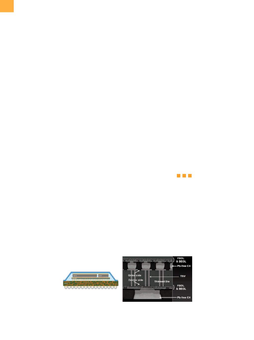
and higher functionality density. An example is given in
Fig. 1, which shows a modern 2.5-D test vehicle including
packaging technologies such as silicon interposer and
micropillar interconnects.
[3]
Figure 1 shows two full-wafer-thickness dice, which
are stacked on a thinned silicon interposer. The dice
package is finally assembled on an organic laminate.
Micropillar technology is used to enable a high-density
interconnection between the dice, while TSV and C4
bumps finalize the overall communication toward the
environment.
The enablement of such packaging solutions not only
requires new processes for TSVs, thin-die manufacturing,
assembly, and test but also a well-defined concept of
process and supply chain, including package FA. When
performing FA of these new package devices, standard
fault isolation techniques such as I-V bench testing,
time-domain reflectometry (TDR), or scanning acoustic
Fig. 1
(a) Example of 2.5-D integrated system-in-package based on interposer technology.
[2]
(b) High-magnification image of
interconnection realization between full die (top), thinned die (middle), and laminate (bottom) using TSV, micropillar,
and thinned-die packaging.
[3]
(a)
(b)