


 27 / 66

edfas.org
27
ELECTRONIC DEVICE FAILURE ANALYSIS | VOLUME 18 NO. 4
If a failure results in an open or short affecting the
interconnections in the top chip, and if electrical access to
the chips is possible, SEM-based FA techniques, combined
with local probing, remainof highvalue. For example, elec-
tron beam absorbed-current imaging was demonstrated
to locate an open in a TSV daisy chain.
[2]
OPTICAL TECHNIQUES
The traditional light-based techniques can also be
applied, if the light can access the region of interest in
or out of a 3-D stack. A lesser-known technique, polaris-
copy,
[5]
was demonstrated to be very sensitive to local
mechanical shear stress variations, as also detected near
TSVs. One can expect that any defect affecting this stress,
suchas voids or delamination, will affect these stress fields
and be detectable. Although promising, the technique is
rather complicated and sensitive to sample conditions;
further research and development is necessary to under-
stand its applicability and limitations.
Time-domain reflectometry, measuring the reflected
signal of a low-amplitude 35 GHz pulse applied into a
conductive circuit, can be used to nondestructively detect
a failure in an interconnection trace. However, this tech-
nique typically could not be used for 3-D stacks because of
its limited sensitivity and resolution. New developments,
usingoptically generated terahertz signals (electro-optical
terahertzpulsed reflectometry), demonstrated that bump-
level failures could be detected in 3-D stacks.
[10]
It was shown several years ago that photon emission
microscopy (PEM) was able to locate a liner breakdown
position in a TSV.
[11]
If access is not possible from the top,
it can be done from the cross section, in some cases. To
allow close inspection of a TSV, as demonstrated in Fig. 5,
an FIB canbe used toopen an area around it, leaving some
silicon around the TSV. The PEM image is then obtained in
situ by rotating the sample with the cross-sectional site
up, allowing analysis of the TSV areawith largemagnifica-
tion, and, in themeantime, probing from the sides. In this
case, the breakdown was found to be near the bottom of
the TSV, at the backside of the copper TSV.
However, this requires locating the leaky TSV first. One
recentlydemonstratedsolution for locatingadefectiveTSV
is the use of light-induced capacitance alteration (LICA),
a type of alternative technique to optical-beam-induced
resistance change, light-induced voltage alteration, or
thermally-induced voltage alteration. In LICA,
[12]
a laser
is scanned across a TSV chain while simultaneously
measuring the capacitance between the chain and the
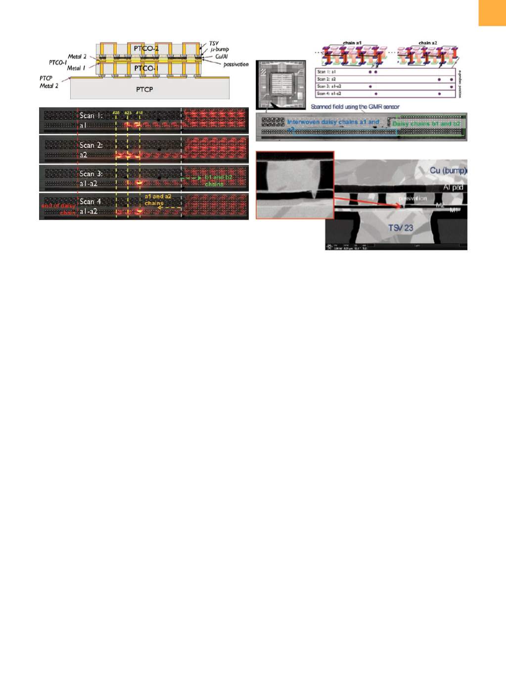
Fig. 4
Failure analysis to find the location of a short between interwoven daisy chains a1 and a2 using magnetic field imaging
(by Neocera) on a 3-D stacked IC sample (from imec) containing two thinned chips (50 µm, PTCO-1 and -2) and one thick
chip (~750 µm, PTCP), interconnected by 5
×
50 µm copper TSVs and microbumps. The sample contains two interwoven
daisy chains (a1 and a2) running betweenPTCP andPTCO-1 (metal 1). Other daisy chains (b1 and b2) run betweenPTCO-1
and PTCO-2 and are not connected to chain a1. MCI is performed to test chains a1 and a2 and between a1 and a2. The
images indicate shorts between the chains and between chains a and b. MCI allowed the short position near TSV No. 23
to be located. Plasma FIB (by FEI) confirmed a failure short between M1 and M2 of PTCO-1 above TSV No. 23.
[7]