


 26 / 66

edfas.org
ELECTRONIC DEVICE FAILURE ANALYSIS | VOLUME 18 NO. 4
26
application domain and the limitations of this technique
is still missing and requires further testing and modeling
of the interaction of sound waves with such samples.
Although currently it is not clear whether small voids
inside a TSV can cause failures, it is preferable to avoid
them, and, for that reason, they must be detected early
in the processing sequence. As such, this is more an
in-line wafer-level metrology requirement than an FA
requirement. For this reason, in addition to GHz-SAM,
other sound-based techniques are being investigated,
such as laser-based acoustic analysis,
[6]
where the signals
obtained fromcontrol TSVs are comparedwith those from
TSVs with voids.
THERMOGRAPHY AND MAGNETIC
CURRENT IMAGING
In addition to x-rays and sound, there are some other
candidates that allow a nondestructive look inside a 3-D
stack: for example, heat andmagnetic fields. A defect that
generates some heat can be located using an infrared
(IR) camera, and, even more, its location in depth can
be found using a lock-in thermography (LIT) system.
[2]
These systems are very sensitive, nondestructive, and
can locate defective spots even through a packaged 3-D
stack. However, one major drawback of LIT is the spatial
resolution, inherent to the IR wavelength, which requires
solid immersion lenses (SILs) to somewhat improve the
resolution. In addition, the depth localization requires
some knowledge of the thermal conduction of the differ-
ent layers in the stack, that is, calibrationand/ormodeling.
Nevertheless, several publications have already demon-
strated various LIT applications for FA of 3-D stacks.
[2]
Although the depth sensitivity may not be adequate to
locate the liner breakdown position along a TSV, it was
recently demonstrated by researchers from FhG CAM
that studying the emission intensity at different focusing
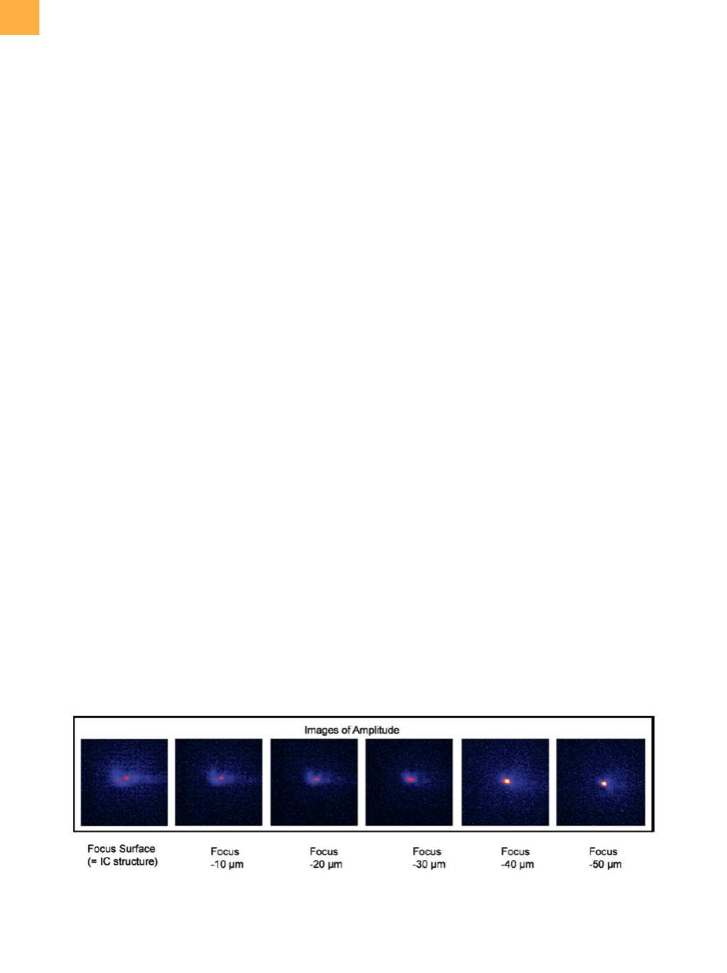
depths can provide additional depth information (Fig. 3).
Magnetic current imaging (MCI), a technique that
received increasing attention due to its potential appli-
cations for 3-D technology,
[7]
can provide a better spatial
resolution (even submicron) than LIT, provided that the
magnetic sensor is close enough to the current path. In
this technique, the in-plane current flow in a sample is
visualizedby detecting the associatedmagnetic field. This
allows, for example, the detection of shorts. A drawback is
that the distance between the current path and the detec-
tor determines the resolution and sensitivity. However,
both can be used to obtain some information about the
location in depth. An example is given in Fig. 4, where the
technique could be used to locate a short in a 3-D stack.
[8]
Further sample preparation was done using a plasma FIB
to analyze the failure site.
It was also demonstrated that the MCI technique can
locate opens. By generating a standing current wave in an
open conductor, thepositionof theopen canbe locatedby
analyzing the decay of the detected magnetic field along
the conductor. As such, this technique could be a solution
to nondestructively detect both opens and shorts in 3-D
SIC stacks. However, further development is once again
required to provide higher sensitivity and better in-plane
and depth resolution. A very promising detector technol-
ogy for this purpose is the one based on detection of the
magnetic spin moment of single-color-center, nitrogen-
vacancy lattice defects in diamond.
[9]
These detectors
promise not only a magnetic sensitivity better than
1 pT/sqrt Hz but also a sub-10 nm spatial resolution,
highly outperforming the currently used superconducting
quantuminterferencedeviceandgiantmagnetoresistance
(GMR) sensors. In addition, these sensors can detect not
only the out-of-plane magnetic field but all field compo-
nents, and they are also sensitive to local temperature
variations. This development may open the way for
improvedMCI on 3-D stacks and also solve some FA issues
of current and future 2-D and 3-D nanotechnology.
Fig. 3
Backside LIT images with SIL taken of a breakdown spot of a 5-µm-diameter, 50-µm-deep copper TSV at different focus
positions. The images clearly indicate that the breakdown is located close to the bottom of the TSV (focus
−
50 µm).
Measurements by C. Grosse and F. Altmann, FhG CAM, Halle, Germany; sample from imec