


 28 / 66

edfas.org
ELECTRONIC DEVICE FAILURE ANALYSIS | VOLUME 18 NO. 4
28
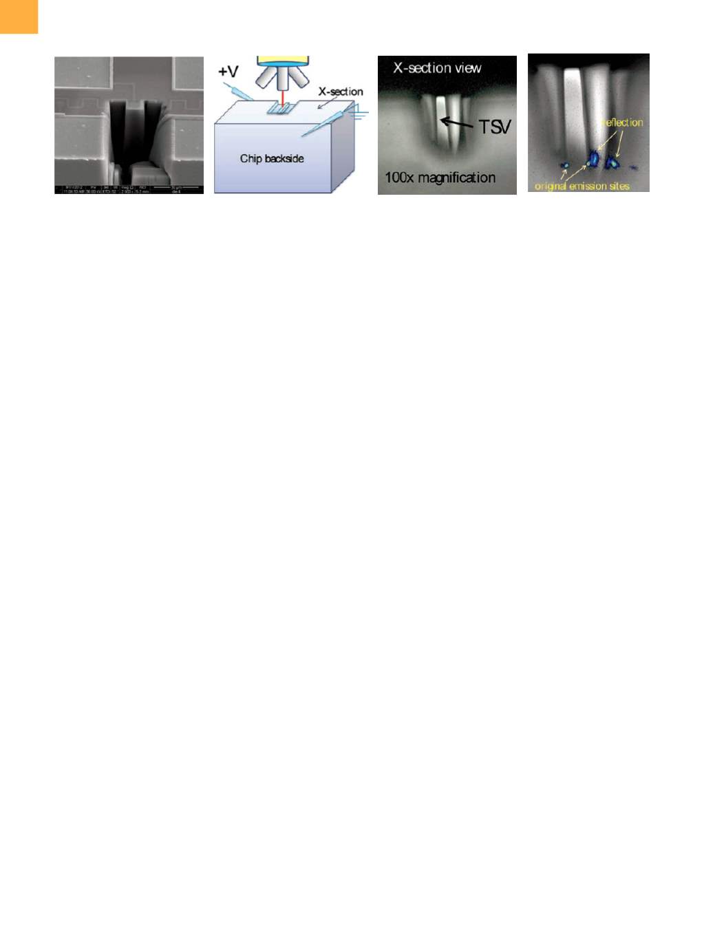
(a)
silicon substrate. Every time the silicon near a connected
TSV is probed by the laser, themeasured capacitance will
change. When a nonconnected TSV is probed, no change
will be detected. This new technique allows easy and fast
localization of an open or short position at the TSV level.
As with all laser-based techniques, one drawback is that
optical access to the TSV region is required, which may
become problematic if several chips are stacked.
CONCLUSIONS AND OUTLOOK
It is clear that although several techniques have been
demonstrated to provide some solutions for FA of 3-D
systems, they all have their limitations. Either they are
limited to the external chips, or they lack in resolution, or
they are too slow. A clever design-for-test will be neces-
sary to partly solve this problem. In addition to further
advances in FA tools, new sample-preparation solutions
are also required, allowing one to singulate chips from a
3-D stack without destroying their functionality and test-
ability. The latter requires additional probing solutions
on TSVs and microbumps.
When looking to the 3-D landscape,
[13]
this technology
is also evolving toward smaller dimensions. Some things
may become easier for the failure analyst, but others
will certainly become more complicated. The 3-D SIC
technology, involving die stacking, die-to-wafer stacks,
and die-to-silicon-interposer stacks, all interconnected
through TSVs (typically 5 µm or larger in diameter), is
evolving to within-die 3-D system-on-chip, involving
parallel front-end-of-line (FEOL) wafer processing and
wafer-to-wafer bonding, where the BEOL of the top
thinned flipped wafer makes direct interconnection to
the one on the bottomwafer. This involves much smaller
TSVs of a few microns in height and a diameter down to
0.5 µm. Future development will bring sequential FEOL
device processing, that is, transistor-level 3-D integration,
also called 3-D IC. Imagine finding the failing transistor
in a chip containing two or more stacked layers of highly
dense nanosized transistors. This 3-D IC technology is
especially promising for vertical devices, and it has already
been demonstrated for 3-D NAND memory devices. It is
clear that FA research and development will remain very
challenging in the future.
REFERENCES
1. F. Lorut, N. Hotellier, S. Lhostis, and F. Ponthenier: “Imaging
Techniques Comparison for Advanced 3Di Devices Characterization,”
41st Int. Symp. Test. Fail. Anal. (ISTFA),
ASM International, Nov. 1-5,
2015, pp. 140-48.
2. F. Altmann, C. Grosse, F. Naumann, J. Beyersdorfer, and T. Veches:
“Failure Analysis Strategies for Multi-Stacked Memory Devices with
TSV Interconnects,”
41st Int. Symp. Test. Fail. Anal. (ISTFA),
ASM
International, Nov. 1-5, 2015, pp. 130-35.
3. T. Wang, I. De Wolf, A. Gu, and R. Estrada: “Application of 3D X-Ray
Microscopy for 3D IC Process Development,” accepted for presenta-
tion at the
13th Int. Wafer-Level Packg. Conf. (IWLPC) 2016,
SMTA and
Chip-Scale Review, Oct. 18-20, 2016.
4. A. Phommahaxay, I. De Wolf, P. Hoffrogge, S. Brand, P. Czurratis,
H. Philipsen, Y. Civale, K. Vandersmissen, S. Halder, G. Beyer, B.
Swinnen, A. Miller, and E. Beyne: “High Frequency Scanning Acoustic
Microscopy Applied to 3D Integrated Process: Void Detection in
Through Silicon Vias,”
Proc. Electron.
Compon. Technol. Conf.
(ECTC),
2013
, pp. 227-31.
5. I. De Wolf, A. Khaled, M. Herms, M. Wagner, T. Djuric, P. Czurratis,
and S. Brand: “Failure and Stress Analysis of Cu TSVs using GHz-
Scanning Acoustic Microscopy and Scanning Infrared Polariscopy,”
41st Int. Symp. Test. Fail. Anal. (ISTFA),
ASM International, Nov. 1-5,
2015, pp. 119-25.
6. R. Mair, M. Kotelyanskii, M. Mehendale, X. Pu, P. Mukundhan, T.
Kryman, M. Liebens, S. Van Huylenbroeck, L. Haensel, A. Miller, E.
Beyne, and T. Murray: Non-Destructive Acoustic Metrology and Void
Detection in 3 × 50 µm TSV,”
27th Ann. SEMI Adv. Semicond. Manuf.
Conf. (ASMC),
IEEE, May 16-19, 2016, pp. 54-59.
7. D. Vallett: “Magnetic Current Imaging Revisited,”
Electron. Dev. Fail.
Anal.,
ASM International, 2014,
16
(4
)
, pp. 26-34.
Fig. 5
In situ localization of the breakdown site of the liner of a 5-µm-diameter, 50-µm-deep copper TSV. (a) Sample prepared
by cleaving and FIB, leaving silicon near the TSV. (b) Schematic showing the sample in the PEM setup and the probing
from the sides. (c) Crosss-sectional microscopy image taken with the PEM setup. (d) Overlay image showing emission
detected near the bottom of the TSV. Some light is reflecting from the side walls of the FIB-cut hole.
(b)
(c)
(d)