


 36 / 66

edfas.org
ELECTRONIC DEVICE FAILURE ANALYSIS | VOLUME 18 NO. 4
36
than for the Ga-FIB. Plasma FIBs are able to maintain a
focused beam even at very large currents in the range of
microamps. Due to this larger range of beam currents,
plasma FIBs are able to achieve much higher milling
rates for larger volumes of material removal. Although
greater damage to the material may be expected with
higher milling rates, the xenon atom, being heavier than
gallium, creates a reduction of surface amorphization by
approximately 24 to 57% on an integrated circuit.
[12]
Also,
xenon, being a nonmetallic, inert element, does not form
intermetallic compounds
[13]
as gallium ions do. Withmain-
taining ahighmaterial-removal rate, higher beamcurrents
must be used on the plasma FIBs. Themain problemwith
using the higher beam currents and hence higher spot
size is the generation of curtaining artifacts. To minimize
these artifacts, the plasma FIB canbe used in combination
with a sample-rocking technique. The sample-rocking
technique uses two alternatingmilling directions that are
a fewdegrees away fromthe traditional vertical direction.
Greatly improved results have been achieved by using
this technique to cross section through silicon vias
[14,15]
and solder bumps.
[15]
CASE STUDIES: APPLICATION OF
EOTPR, X-RAY, AND PLASMA FIB FOR
ELECTRICAL OPEN DETECTION
Because there have been many publications and dis-
cussions about the operational principle, performance,
and comparison of SQUID and LIT, this article will focus
on the application of EOTPR, 3-D x-ray, and plasma FIB
specifically for the detection of electrical opens.
SAMPLE DESCRIPTION
To demonstrate the potential and advantage of the
introduced FA techniques, a Globalfoundries test vehicle
is investigated. Figure 5 depicts a schematic buildup
showing a standard 20 nm flip-chip stacked dice sample
with interconnects covered with mold compound.
OPEN DETECTION ON DIE-SUBSTRATE LEVEL
Todemonstrate the FAflowadvantage of the proposed
methods, a samplewith an electrical open in an unknown
x,y,z
location within the package has been used. After
confirming the defect signature electrically, EOTPR is
applied without any sample preparation. The results are
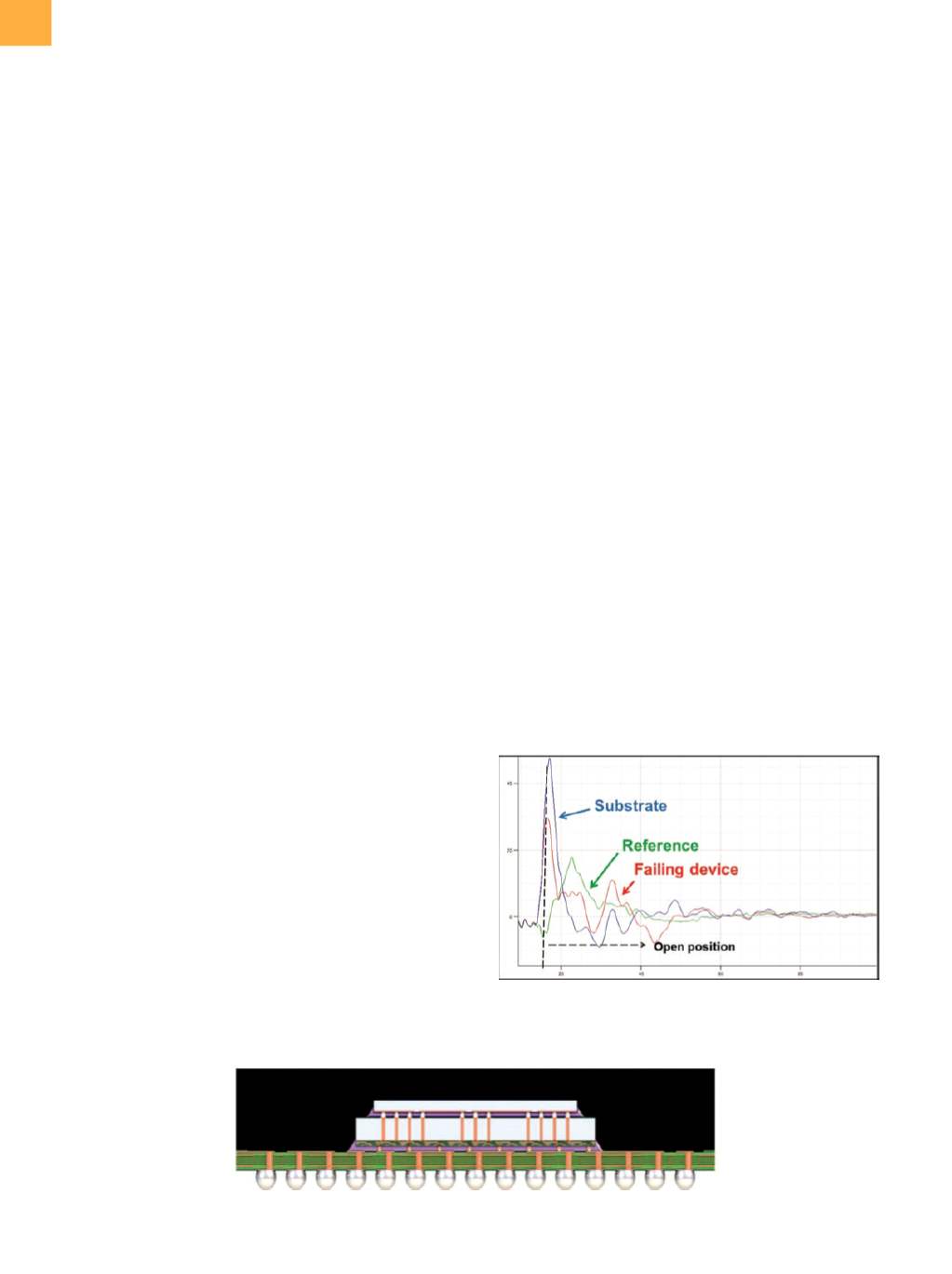
plotted in Fig. 6. By comparing the failing sample to both
a reference and a bare laminate sample, an additional
peak can be observed.
The comparison in Fig. 6 clearly shows that the defect
can be suspected in or close to the die-substrate interface.
After reviewing the sample layout, the
z
-position of the
defect is estimated, while
x
and
y
are still to be deter-
mined. For that purpose, the sample is investigated by
3-D x-ray (Fig. 7).
Reviewing the generated 3-D model, a difference in
the fail-related microbump can be observed compared
to the surrounding connections. By using the virtual
cross-section feature, the root cause can be identified
as a nonwetting bump issue. For the final step of the FA,
the isolated defect position is investigated with plasma
FIB. Therefore, the sample package is thinned from
the laminate side. To ensure the defect is unharmed,
sample preparation is stopped within the laminate, and
the plasma FIB is used to cross section through the die-
substrate interface (Fig. 8).
Cross sectioning the isolated defect area confirms
the obtained 3-D x-ray results. Reaching the center of
the bump, no connection between the microbump and
substrate is visible.
Instead, the original postbump shape
Fig. 5
Schematic drawing of wide I/O on logic dice with TSV
Fig. 6
EOTPR results on failing device, reference, and
bare substrate indicate a defect located in the die-
substrate interface
(continued from page 34)
EMERGING TECHNIQUES FOR 2-D/2.5-D/3-D PACKAGE FAILURE ANALYSIS