


 37 / 66

edfas.org
37
ELECTRONIC DEVICE FAILURE ANALYSIS | VOLUME 18 NO. 4
is still visible, indicating a nonwet issue during package
assembly.
OPEN DETECTION ON DIE-DIE LEVEL
In a second case study, FA is conducted on the same
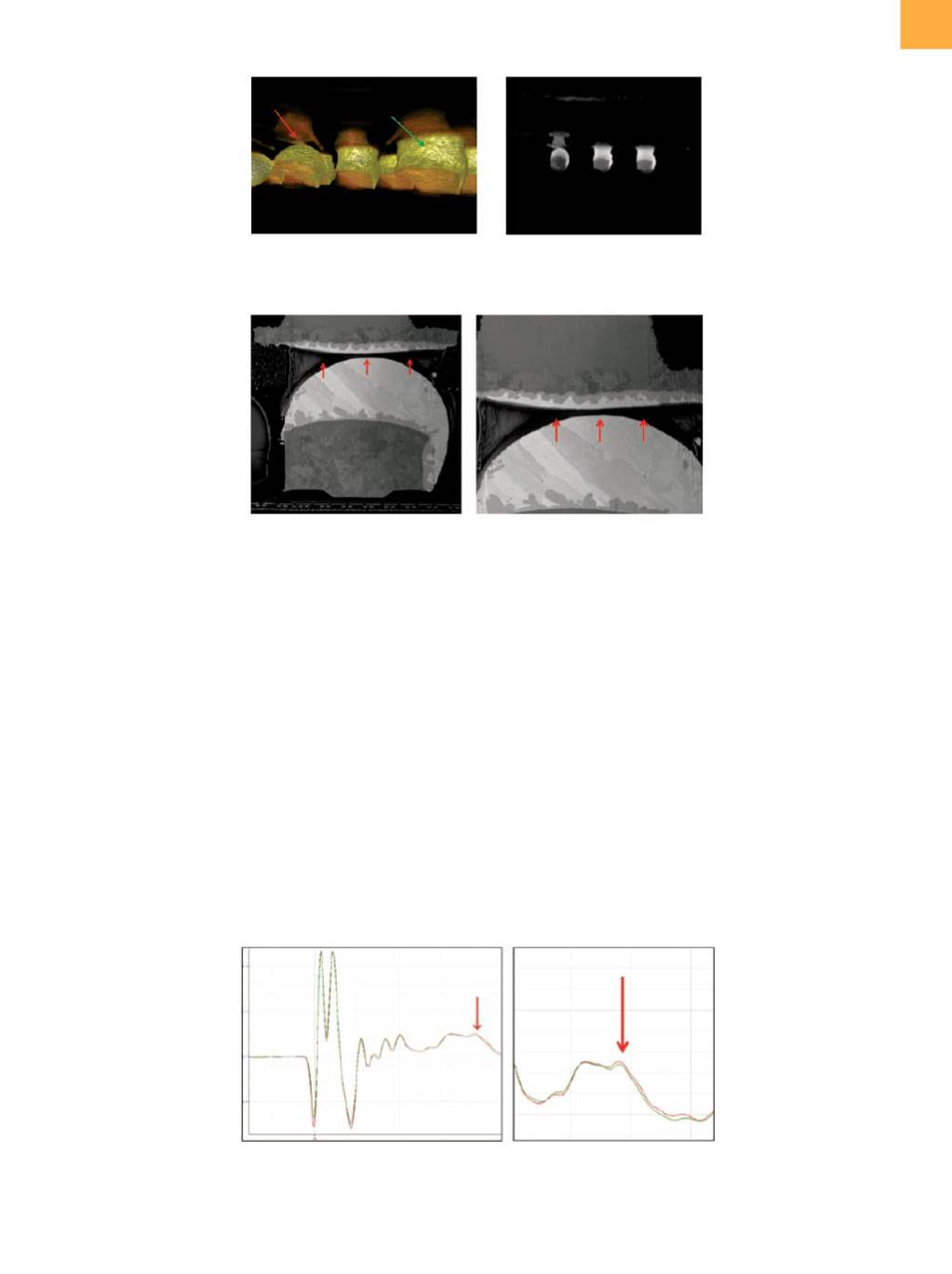
package product. Here, multiple electrical opens have
been detected after package assembly. Again, EOTPR is
used as the first analyzing method (Fig. 9).
As the signal travels through theball-gridarray contact,
laminate, and copper pillar region, an identical signature
can be observed for reference and failing devices. As the
signal enters the die-die interface, a slight difference is
noticeable. This led to the working theory that the open
is present within the TSV/microbump region. For further
analysis, the region of interest was inspected by 3-D x-ray.
As can be seen in Fig. 10, the root causewas identified as a
general misalignment that resulted in partial or fully open
interconnects between the TSV andmicrobump features.
For final confirmation and additional data gathering,
the area of interest was cross sectioned by plasma FIB.
Using the high-beam current advantage, a direct cut was
made from the sample surface through the top die, inter-
connect interface, and bottom die (Fig. 11).
The FIB cross section through the TSV center for both
reference and failing samplesmakes the failure root cause
clearly visible. While the reference sample shows a solid
interconnection between top die, microbump, and TSV,
the failed sample ismissing this connection. Furthermore,
(a)
(b)
(a)
(b)
Fig. 7
(a) 3-D x-ray and (b) virtual cross section identify the root cause of the electrical open as a nonwet microbump.
Fig. 8
Plasma FIB cut through a failing bump confirms the 3-D x-ray results and root-cause theory of an unlandedmicrobump.
Fig. 9
(a) EOTPR measurement overview and (b) high magnification of reference (green) and failing (red) device signatures.
A slight difference is noticeable after the signal passes the ball-grid array contact and laminate.