


 38 / 66

edfas.org
ELECTRONIC DEVICE FAILURE ANALYSIS | VOLUME 18 NO. 4
38
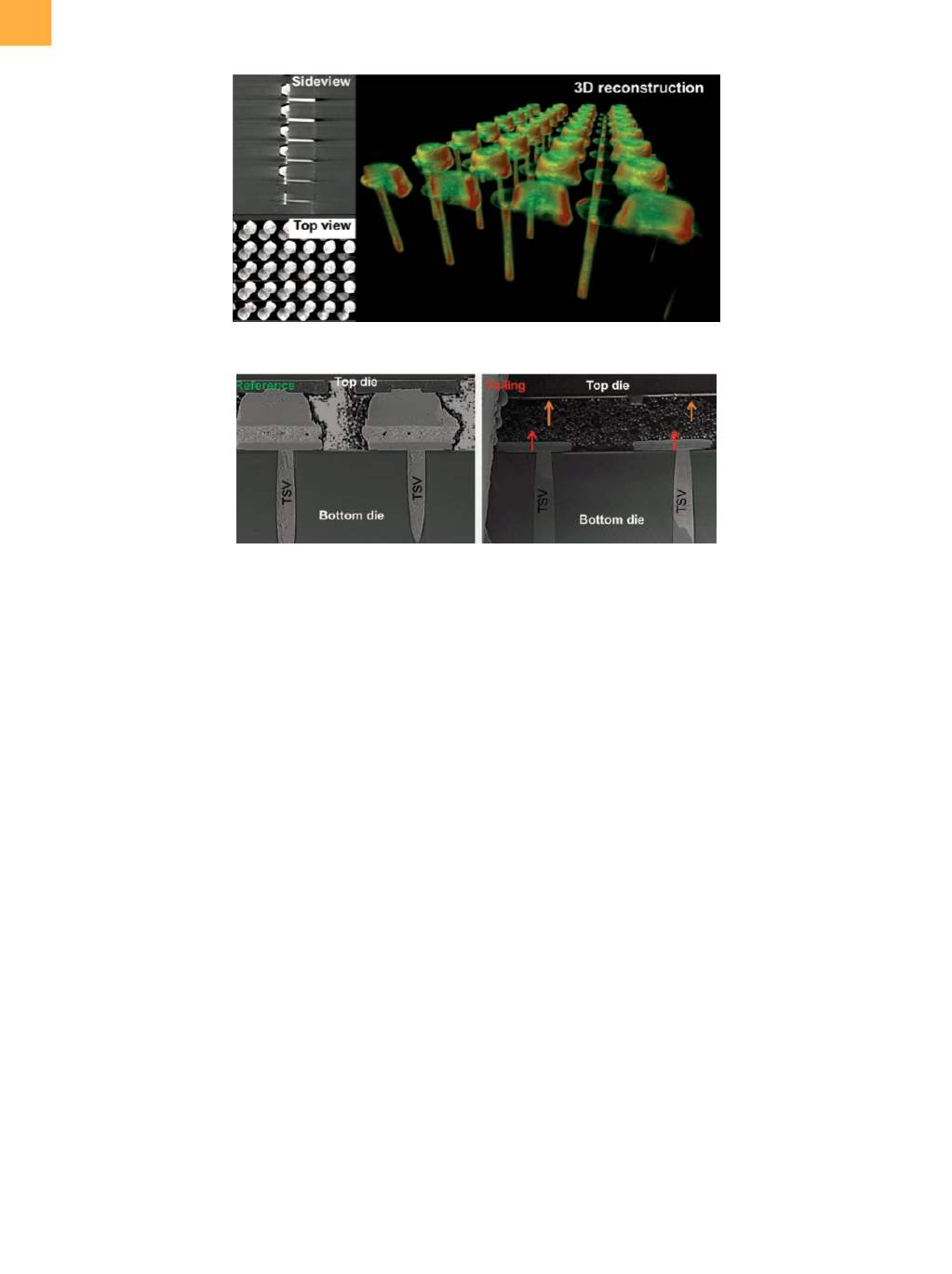
no bump pad can be seen on the top die side, which
confirms a die-die misalignment as the most likely root
cause. By using EOTPR, x-ray, and plasma FIB, this FA case
was able to be closed within 5 to 8 h, with sufficient data
information for follow-up questions and requirements.
CONCLUSION
In this article, the authors have attempted to reflect
on the emerging issue of how high-quality package FA
can be provided for increasingly complex 2-D, 2.5-D, and
3-D package products. After identifying pressing issues
and potential bottlenecks with the state-of-the-art FA
flow, the methods of EOTPR, 3-D x-ray, and plasma FIB
have been introduced. An integration flow for specific FA
cases has beenproposed anddemonstratedon twodiffer-
ent case studies. Hereby, the FA results confirm the high
potential of all three techniques and additionally enable
the opportunity for a fully nondestructive FA approach.
From a technical point of view, the following advantages
can be observed:
• EOTPR allows for early detection of the defect
z
-posi-
tion with the sample fully functional and unprepared.
This enables further control over product-specific FA
flow optimization.
• 3-D x-ray helps indicate the defect mechanism before
physical failure analysis. Using the virtual cross-sec-
tioning feature, the defect was isolated by 3-D, which
allowed optimum navigation for the cross section. In
addition, a combination of EOTPR and 3-D x-ray with
a defect database opens the opportunity for a fully
nondestructive package FA.
• Plasma FIB over conventional cross-sectioning tech-
niques removes the risk of potential preparation
artifacts such as cracks, foreign materials, or damage
(slurry, acid, etc.). It also significantly reduces the
turnaround time compared to Ga-FIB.
Considering these methods from a high-volume per-
spective, further optimization is required. In all cases,
standard setups allow only one sample investigation at
a time. While a multitool option is both cost and mainte-
nance extensive, further development focus is needed on
measurement automation.
REFERENCES
1. “3D IC Integration and TSV Interconnects—2010 Market Analysis,”
Yole Development, 2010.
2. J. Oswald et al.: “2.5D Packaging Solution—From Concept to Plat-
form Qualification,”
17th Electron. Packg. Technol. Conf.,
2015,
pp. 1-7.
(a)
(b)
Fig. 10
3-D x-ray results showing a misalignment between microbumps and TSV features
Fig. 11
Plasma FIB cut through x-ray-investigated area for (a) reference and (b) failing devices. High-magnification scanning
electron microscopy imaging confirmed missing die-die interconnection as the root cause.