


 20 / 66

edfas.org
ELECTRONIC DEVICE FAILURE ANALYSIS | VOLUME 18 NO. 4
20
herein are those of the authors and should not be inter-
preted as necessarily representing the official policies
or endorsements, either expressed or implied, of IARPA,
AFRL, or the U.S. Government.
REFERENCES
1. S. Kasapi, C.-C. Tsao, K. Wilsher, W. Lo, and S. Somani: “Laser Beam
BacksideProbingof CMOS IntegratedCircuits,”
Microelectron.Reliab.,
1999,
39
(6), pp. 957‑61.
2. J.A. Kash and J.C. Tsang: “Dynamic Internal Testing of CMOS Circuits
Using Hot Luminescence,”
IEEE Electron Dev. Lett.,
1997,
18
(7), pp.
330-32.
3. F. Stellari, P. Song, J.C. Tsang, M.K. McManus, and M.B. Ketchen:
“Testing and Diagnostics of CMOS Circuits Using Light Emission
from Off‑State Leakage Current,”
IEEE Trans. Electron Dev.,
2004,
51
(9), pp. 1455‑62.
4. A. Weger, S. Voldman, F. Stellari, P. Song, P. Sanda, andM. McManus:
“Transmission Line Pulse Picosecond Imaging Circuit Analysis
Methodology for Evaluationof ESDand Latchup,”
Int. Rel. Phys. Symp.
(IRPS),
2003, pp. 99‑104.
5. S. Kasapi and G.L. Woods: “Voltage Noise and Jitter Measurement
Using Time‑Resolved Emission,”
Int. Symp. Test. Fail. Anal.
(
ISTFA),
2006, pp. 438‑43.
6. F. Stellari, A. Tosi, and P. Song: “Switching Time Extraction of CMOS
Gates Using Time‑Resolved Emission (TRE),”
Int. Rel. Phys. Symp.
(IRPS),
2006, pp. 556‑73.
7. S. Polonsky and K.A. Jenkins: “Time‑Resolved Measurements of
Self‑Heating in SOI and Strained‑Silicon MOSFETs Using Photon
EmissionMicroscopy,”
IEEE ElectronDev. Lett.,
2004,
25
(4), pp. 208‑10.
8. S. Polonsky, M. Bhushan, A. Gattiker, A. Weger, and P. Song: “Photon
Emission Microscopy of Inter/Intra Chip Device Performance
Variations,”
Eur. Symp. Reliab. Electron Dev., Fail. Phys. Anal. (ESREF),
2005, pp. 1471-75.
9. R.H. Hadfield: “Single-Photon Detectors for Optical Quantum
Information Applications,”
Nature Photon.,
2009,
3
, pp. 696-705.
10. A. Bahgat Shehata, F. Stellari, A. Weger, P. Song, V. Anant, K. Sunter,
K.K. Berggren, T. Lundquist, andE. Ramsay: “Ultra-LowVoltage Time-
Resolved EmissionMeasurements from32 nmSOI CMOS Integrated
Circuits,”
Proc.40thInt.Symp.Test.Fail.Anal.(ISTFA),
2014, pp. 415‑21.
11. A. Bahgat Shehata and F. Stellari: “Tuning of Superconducting
Nanowire Single‑PhotonDetector Parameters for VLSI Circuit Testing
Using Time‑ResolvedEmission,”
SPIEPhotonicsWest, Proc. SPIE 9370,
2015, article no. 93702Z.
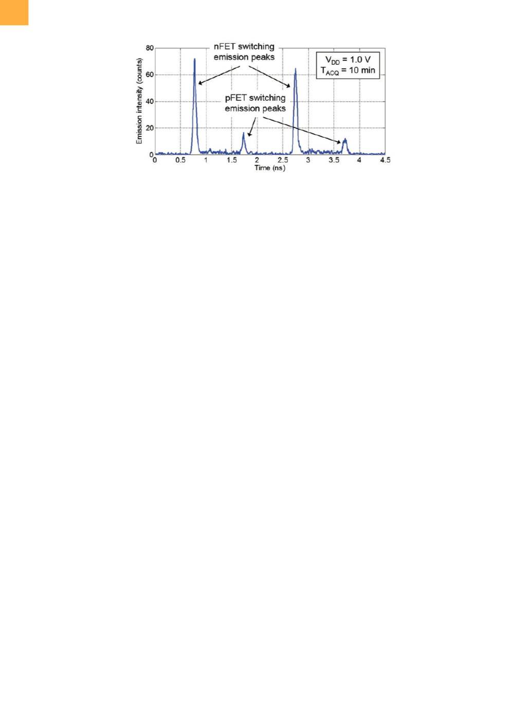
The frequency of the ring operated at 1 V is 508 MHz,
leading toaperiodof approximately 2ns. Due to the scaled
feature size, light can be collected fromboth the
n
FET and
p
FET in a single measurement, as shown in Fig. 7.
CONCLUSIONS
Notwithstanding the continuous advances of
design-for-manufacturing and design-for-test features,
time-resolved optical probing techniques remain an
indispensable tool to increase the accuracy and speed
of fault localization. Novel detectors, such as the SSPD,
have become available to return light to TRE techniques
that can aid or replace LVP in situations where complete
noninvasiveness is necessary. The detector and the tech-
nique have been demonstrated for scaled nodes such as
14 nmFinFET SOI and for ultra-low-power supply voltages
down to 0.4 V.
ACKNOWLEDGMENTS
The authors would like to acknowledge and thank
many people from IBM T.J. Watson Research Center,
Massachusetts Institute of Technology, Photon Spot,
and FEI for useful discussions, suggestions, and support,
including Herschel Ainspan, Seongwon Kim, Christian
Baks, Marc Taubenblatt, Mehmet Soyuer, Kristen
Sunter, Karl Berggren, Vikas Anant, Euan Ramsay, Herve
Deslandes, Ted Lundquist, and Dave Schleh.
The work described in this paper was done within a
project supported by the Intelligence Advanced Research
Projects Activity (IARPA) via Air Force Research Laboratory
(AFRL) contract number FA8650-11-C_7105. The U.S.
Government is authorized to reproduce and distribute
reprints for governmental purposes notwithstanding any
copyright annotation thereon.
Disclaimer: The views and conclusions contained
Fig. 7
TRE waveform acquired from an inverter of a 100‑stage IBM 14 nm FinFET SOI ring oscillator. The light is collected from
a single inverter. The switching emission peaks from both the
n
FET and
p
FET are visible.
(continued on page 22)