


 19 / 66

edfas.org
19
ELECTRONIC DEVICE FAILURE ANALYSIS | VOLUME 18 NO. 4
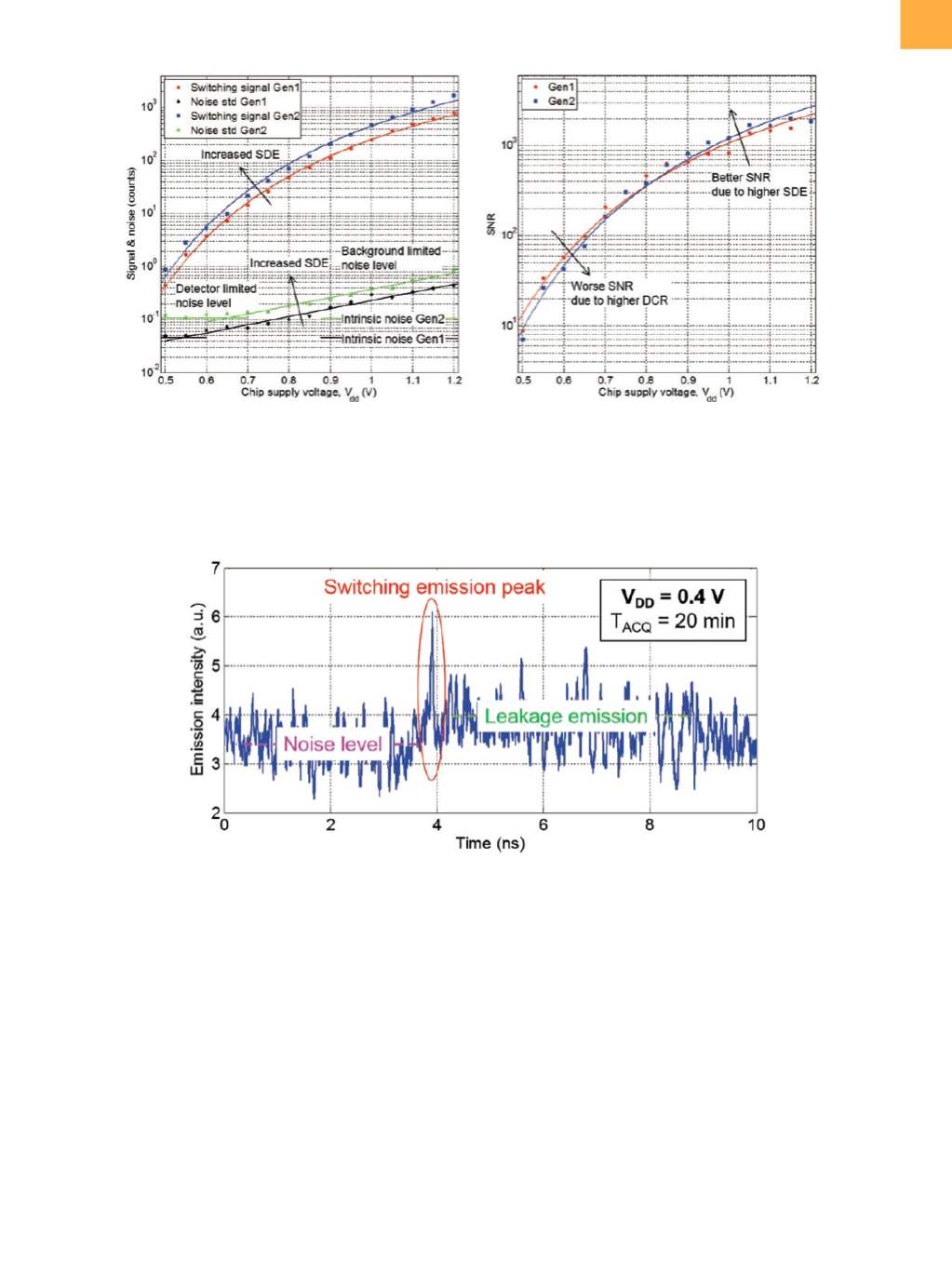
(a)
signal and the noise are higher. (In fact, themeasurement
noise increases with voltage because some light from
the neighboring FETs is collected as well.) The resulting
signal-to-noise ratio (SNR) is shown in Fig. 5(b). The sec-
ond-generation SSPD yields a better SNR at high voltage
due to its improved detection efficiency, but it also has
worse performance at low voltage due to its higher DCR.
It should be noted that the switching emission peak
amplitude strongly depends on the temporal response
(i.e., jitter) of the system(detector
+
electronics): the lower
the jitter, the narrower and taller the peak. Therefore, it is
crucial to optimize the SSPD front‑end electronics. With
careful tuning of themain systemknobs that are available
to the user,
[11]
it is possible to acquire TRE waveforms in
just a few seconds at a nominal supply voltage of 0.9 V
and in approximately 20min at aworld record low-supply
voltage of only 0.4 V
[10]
(Fig. 6).
APPLICATION TO SCALED
TECHNOLOGY NODES
The capabilities of TRE have been demonstrated on
scaled technology nodes such as a ring oscillator fabri-
cated in 14 nm FinFET technology. The TRE waveform
acquired fromone of the inverter stages is shown in Fig. 7.
Eachminimum-sized transistor has five fins, and the sepa-
ration between
n
FET and
p
FET of each inverter is 86 nm.
Fig. 5
(a) Switching emission signal and noise as a function of chip supply voltage for two different generations of SSPD.
[10]
The noise at low voltage is limited by the detector noise, while at high voltage it is limited by the background (i.e., light
coming from neighboring devices). (b) Signal-to-noise ratio (SNR) as a function of supply voltage for the two detec-
tors.
[10]
SDE, system detection efficiency; DCR, dark-count rate
Fig. 6
Ultra‑low-voltage TRE measurement acquired from an inverter chain fabricated in IBM SOI 32 nm technology.
[10]
The
leakage emission can be distinguished from the noise level, and the switching emission peak can be easily identified.
(b)