


 17 / 66

edfas.org
1 7
ELECTRONIC DEVICE FAILURE ANALYSIS | VOLUME 18 NO. 4
linear dependency on circuit voltage. However, the laser
may also alter timing characteristics of the device. As
device geometries shrink, the number of injected car-
riers required to affect the operation of the circuit also
decreases, thus making it possible to cause catastrophic
damage to the device. Furthermore, when multiple
switching transistors lie inside the focused laser spot,
the acquired signal becomes complex to interpret due to
the constructive and destructive contributions. Different
transistors modulate the reflected beam with different
phase conditions, and so the signal is not strictly addi-
tive; in some cases, the modulation may be cancelled
out almost completely through two opposing phase con-
ditions. Usually, LVP is used in combination with a laser
scanning microscope, allowing the user to test a portion
of the chip (laser voltage imaging).
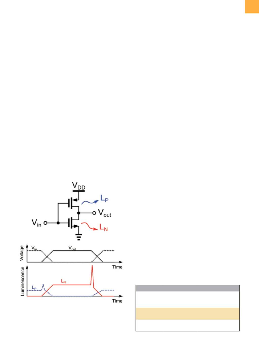
On the other hand, time‑resolved emission (TRE),
[2]
also known as picosecond imaging circuit analysis (PICA),
is a truly noninvasive technique, based on the collection
of intrinsic near-infrared (NIR) photon emission from
CMOS transistor channels (Fig. 1b). This technique allows
one to detect both the logic state of the gates and the
switching events (Fig. 2). Considering a digital gate, a
faint but continuous emission is produced by the leakage
current during off-state with the gate grounded and the
drain high. No emission is produced when the transistor
is in ohmic state with drain and source shorted; a short,
bright emission peak is produced during a switching
event, because the transistor momentarily undergoes
saturation. Contrary to LVP, TRE signals are always addi-
tive, meaning that if two different devices are emitting
close to each other, the resulting collected waveform
will have the signals from both devices. Time‑resolved
emission measurement of off‑state leakage
[3]
and carrier
recombination have led to completely new applications,
such as latch-up ignition,
[4]
power supply noise,
[5]
slew-
ratemeasurement,
[6]
self-heating estimation,
[7]
variability
characterization,
[8]
and so on. However, during the last
decade, the use of TRE has been significantly limited
by two critical factors: sensitivity (as a combination of
detection efficiency, detector noise, and spectral cover-
age) and time resolution. As the chip supply voltage is
reduced, the intrinsic photon emission decreases expo-
nentially, making the use of TRE techniques challenging
for low‑power ICs. Luckily, novel photodetectors such as
the superconducting single‑photondetector (SSPD)
[9]
that
have become available in recent years have helped return
the light to theTRE technique, due to lower noise (fewdark
counts per second) and better jitter (approximately 30 ps
full width at half‑maximum). It must be noted that at the
present time, TRE allows one to probe single points in a
chip; however, lower acquisition times are needed with
better detectors, and raster scanning can be applied to
cover at least a small area of the device under test (DUT).
Moreover, 2-D detectors are currently being developed,
which will enable parallel acquisition.
SUPERCONDUCTING
SINGLE‑PHOTON DETECTOR
An SSPD is ameandermade of superconductingmate-
rial (in this case, NbN shaped in a 9-µm-diameter circle
to match the single-mode fiber used to collect the light;
Fig. 2
Example of luminescence signal (L) from a simple
inverter gate. With TRE, it is possible to retrieve both
the logic state of the gate (the gate is leaking when
it is off) and when it turns on (in correspondence of
the switching emission peak).
Table 1 Comparison of LVP and
TRE techniques
LVP
TRE
Invasive
Yes—may alter
circuit behavior and
cause damage
No—completely passive
Time
resolution
~1 ns
~30 ps
Power supply
dependency
Linear
Exponential