


 12 / 66

edfas.org
ELECTRONIC DEVICE FAILURE ANALYSIS | VOLUME 18 NO. 4
12
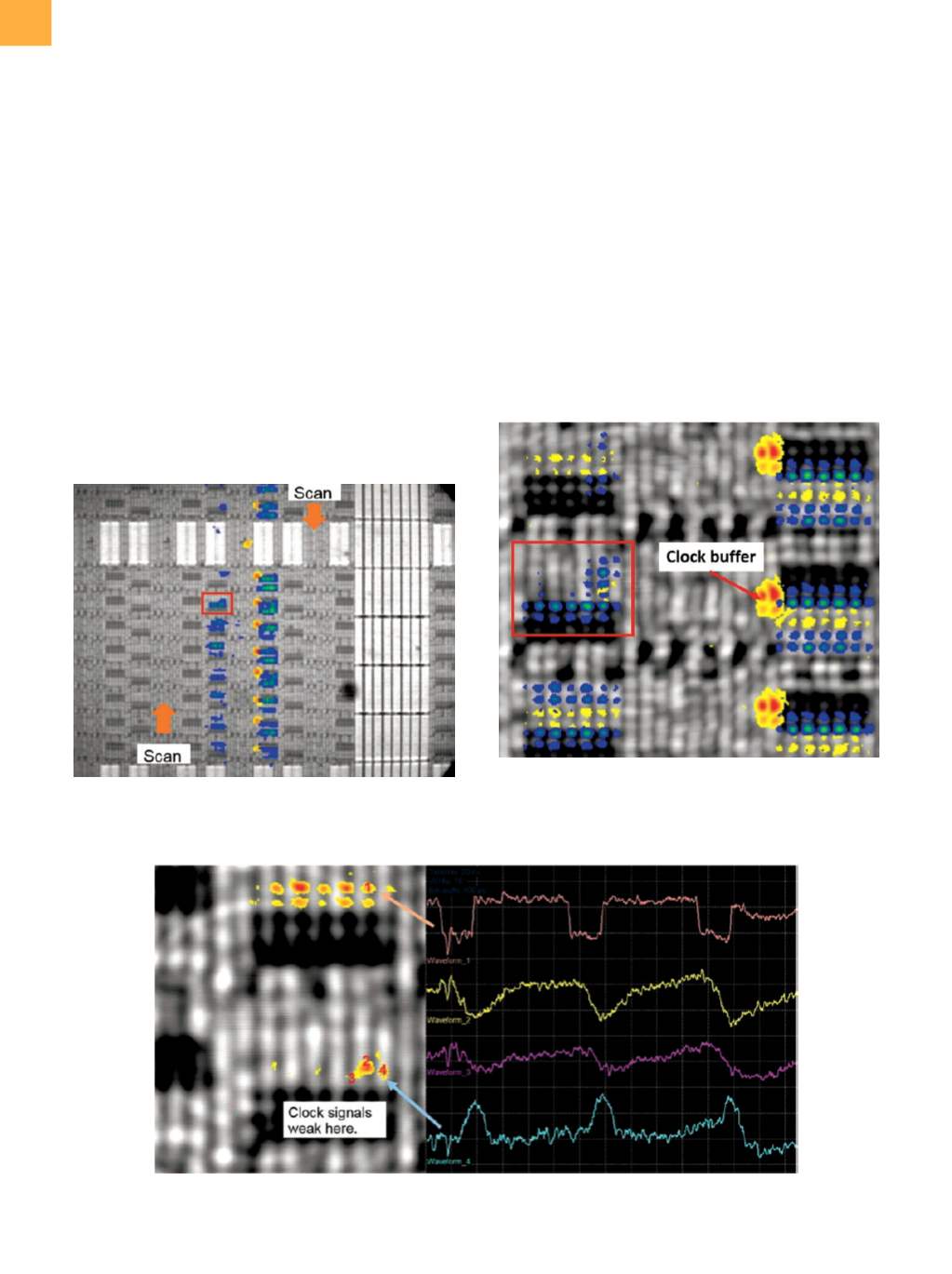
all six scan chains in the same pack. These six latches are
clocked by the same clock buffer and also are loaded by
the same data buffer during preload mode (Fig. 10). The
chip was subject to LVI analysis. The LVI image, shown in
Fig. 11 with the clock signal in yellow and the data signal
in blue, revealed that the data signal stopped at the latch
callout. Figure 12 is a higher-magnification LVI image at
the latch callout. It further showed that the clock signal is
very weak in the latch callout. However, the clock signal
in the clock buffer is still very strong. Furthermore, the
latches close to the clock buffer have some data signal,
while the latches far fromthe clock buffer do not have any
data signal passing through. This implied that the signal
became degraded between the clock buffer and the latch
callout. Laser voltage probingwas employed to check the
clock signal in the latch callout (Fig. 13). Comparing the
waveform from point 1 to the waveforms from points 2,
3, and 4, it was clearly seen that the waveforms at points
2, 3, and 4 were degraded. Based on layout tracing, the
suspected defect was believed to be a highly resistant via
in the interconnect from the clock buffer to the input of
the latch callout. A subsequent focused ion beam (FIB)
cross section on the suspected highly resistant via found
a hollow V2 (Fig. 14).
SCAN CHAIN SINGLE-LATCH SOFT FAILURE
The third case study is a scan chain single-latch soft
failure. The latch passed at high voltage but failed at low
voltage. Although routine PFA on a scan chain single-latch
hard failure can find a defect in most cases, a soft failure
LVI AND LVP APPLICATIONS IN IN-LINE SCAN CHAIN FAILURE ANALYSIS
(continued from page 10)
Fig. 11
LVI image of the six scan chainswith clock-type failure
in a pack. The red square indicates the latch callout
position.
Fig. 12
Magnified LVI image of Fig. 11 shows a strong clock
signal at the clock buffer and some data signals for
the latches close to the clock buffer, and no data
signals for the latches far from the clock buffer.
Fig. 13
LVP waveforms of the input clock circuitry inside the latch callout show a weak clock signal compared to the one from
the reference latch.