


 10 / 66

edfas.org
ELECTRONIC DEVICE FAILURE ANALYSIS | VOLUME 18 NO. 4
10
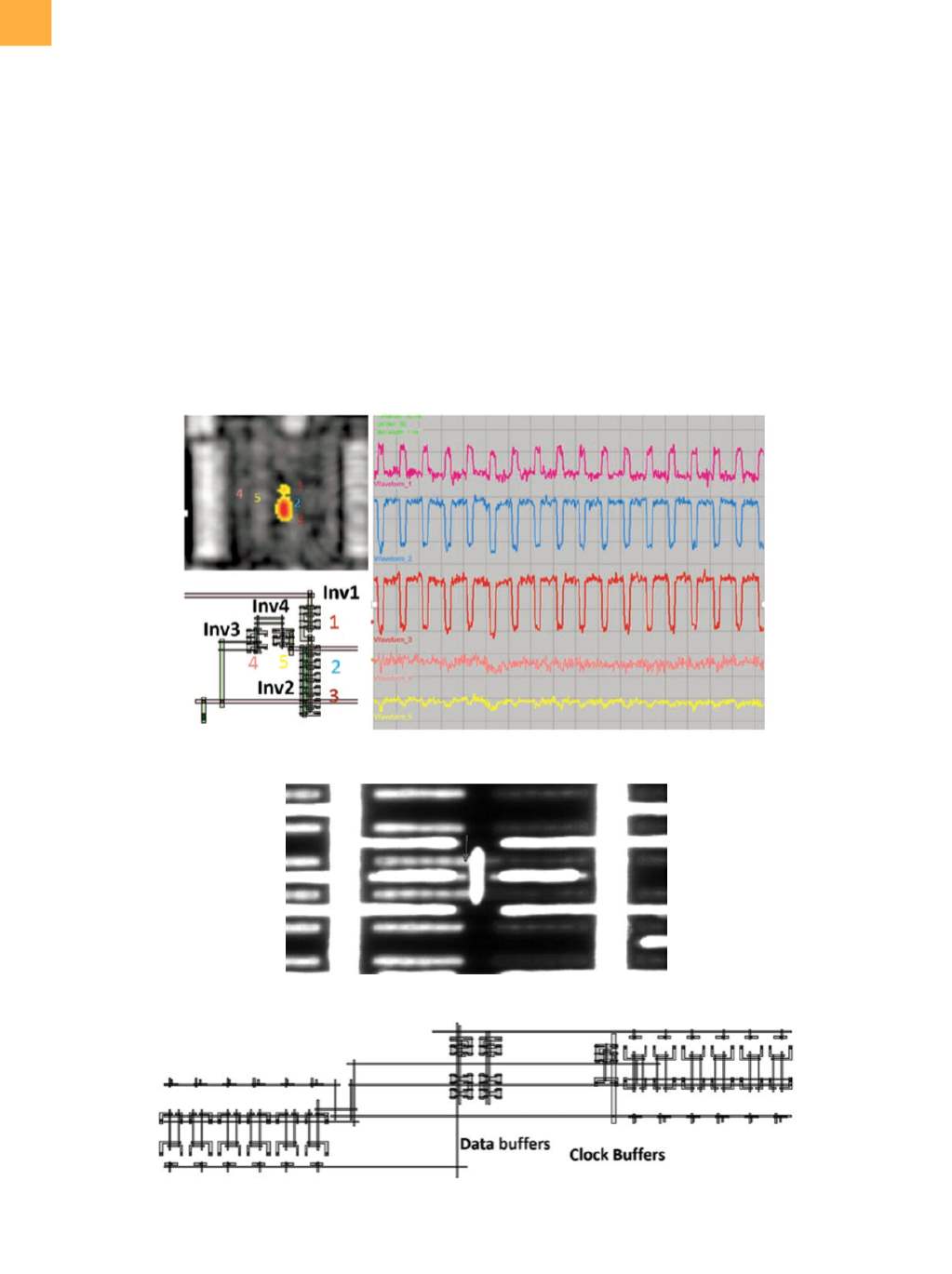
signal propagation was broken (Fig. 7). Further compari-
son of the LVI signals from the clock buffers for blocks 1,
2, and 3 showed that many LVI signals were missing from
the clock buffer for block 2, compared to those from the
clock buffer for block 1, and no LVI signal came out from
the clock buffer for block 3. This indicated that the D clock
signal was supposed topropagate fromthe clockbuffer for
block 1, to the clock buffer for block 2, to the clock buffer
for block 3, and so on; however, it stopped at the clock
buffer for block 2. With layout tracing, it was found that
there are several cascaded inverters for each clock buffer
(Fig. 8). Laser voltage probingwas employed to collect the
waveformfromeach inverter. Thewaveforms shownat the
right in Fig. 8 were collected from five points. Waveform
1 was from inverter 1, and waveforms 2 and 3 were from
inverter 2 because of a long inverter. Waveforms 4 and 5
were from inverters 3 and 4, respectively. It clearly showed
that the clock signal got stuck starting at inverter 3. The
subsequent PFA showed a short between the source/
drain contact and the gate contact at inverter 3, leading
to a malfunction of this inverter, which was responsible
for the skip test scan chain failure (Fig. 9).
SCAN CHAIN CLOCK-TYPE FAILURE
The second case study is a clock-type failure for a
main scan chain pack, namely the same latch callout for
(continued on page 12)
Fig. 8
LVP waveforms collected from five points marked in the layout clip of the cascaded inverters
Fig. 9
SEM image showing a short between the source/drain contact and the gate contact at inverter 3
Fig. 10
Layout tracing that shows these latches at the same position in different scan chains in a pack are sharing the same
clock buffer and data buffer
LVI AND LVP APPLICATIONS IN IN-LINE SCAN CHAIN FAILURE ANALYSIS
(continued from page 8)