


 6 / 66

edfas.org
ELECTRONIC DEVICE FAILURE ANALYSIS | VOLUME 18 NO. 4
6
design latch. Most latches are representative of the ones
used in product logic. The length of the scan chains/
blocks varies according to the size of a given latch type.
The smallest group of latches that can be tested indepen-
dently is a pack, when all but one pack are skipped across
all blocks with the help of a skip test scan chain. Between
subsequent latches, a mux-2 circuit is implemented to
enable two modes: serial scan, where data are fed from
the previous latch, and preload mode, where data are
preloaded from a buffer.
The in-line scan chain logic macro can be operated in
three differentmodes: flush, scan, or preload. The first two
modes are used to test the functionality of the macro. In
the flush mode, all clocks are kept high, and serial data
ripple through the latches from the scan input pins to
the scan output pins. For the scan mode, the serial data
are scanned through the latches by clocking the latches’
master and slave clocks.
The preload mode is used to electrically identify the
failing latch in the event of a failure during the flush/
scan mode operations, that is, when the data observed
on the scan output pins do not match the expected data
based on the pattern exercised on the scan input pins. In
the preload mode, data are loaded simultaneously in all
latches through the mux-2 circuit according to two pos-
sible sequences of 0101… or 1010…, respectively. These
are referred to as checkerboard and reverse checkerboard
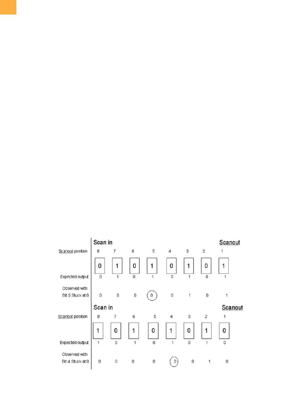
patterns. As an example, in Fig. 4 the chain has a total
of eight latches. The preloaded checkerboard pattern
was “01010101,” and the observed scan-out pattern was
“00000101.” After comparing these two patterns, the first
suspected failing latch was found to be latch No. 5 from
the scan-out pin. However, when the reverse checker-
board pattern “10101010” was preloaded, the observed
scan-out pattern was “00000010.” It suggested that the
first failing latch was latch No. 4 from the scan-out pin,
and latch No. 4 with a stuck-at-0 fault also explained the
observed scan-out pattern in the checkerboard preload
test. With the checkerboard and reverse checkerboard
tests, the first failing latch was identified to be latch No.
4 from the scan-out pin. In summary, the first failing latch
is identified as the closest failing latch from the output
pins of both complementary checkerboard and reverse
checkerboard patterns.
The aforementioned latch callout identificationproce-
dure can be simplified with graphical display, which has
been described in detail in Ref 14. Figure 5(a) shows an
example of a single-latch failure, while Fig. 5(b) shows a
clock-type failure. In Fig. 5, awhite pixel indicates themea-
sured data matches the expected data, while a dark pixel
indicates the measured data do not match the expected
data. The first datum scanning out from the scan chain is
displayed at the extreme left. The first dark pixel counting
from the left, whether in a checkerboard row or a reverse
Fig. 4
Example of eight-latch scan chain with latch No. 4 stuck at 0 identified by checkerboard pattern (top) and reverse
checkerboard pattern (bottom) preload tests
(continued on page 8)