


 5 / 66

edfas.org
5
ELECTRONIC DEVICE FAILURE ANALYSIS | VOLUME 18 NO. 4
the silicon backside while the DUT is exercised. The laser
beam reflects from the interface between the backside
silicon and the active regions, such as drain and channel.
The reflected laser beamhas amodulated amplitude and
phase. Because the modulated amplitude is dependent
on the transistor state, namely the electrical field in the
drain area and/or the free carrier density in the channel,
extraction of the modulated amplitude of the reflected
laser beam indicates the states of the transistor, onwhich
the laser beam is focused. Figure 1 is a simplified LVP sche-
matic. Initially, the application of LVPwasmainly in design
debug and device characterization, rather than fault isola-
tion. This is because the waveforms obtained with LVP at
any given time come from a particular point, namely one
transistor or one node. To search for a defective transistor
or node, it is necessary to probe each transistor or node
one by one. It is time-consuming.
Rather than acquiring data at a single point on a DUT
in the time domain, LVI
[7-9]
collects data in the frequency
domain from numerous points in the field of view on a
DUT. The LVI technique rasters a laser beamacross an area
of a DUT through the backside silicon. At each point, the
reflected laser beam is modulated in both amplitude and
phase at the switching frequency of the transistor under
the area on which the laser is focused. The modulated
reflected laser beam shoots on a photodetector with
transimpedance and radio-frequency amplifiers, and then
amodulated electrical signal is generated. After spectrum
analysis, a signal with a particular frequency is generated.
The signal synchronizes with the laser scan and forms an
LVI image, overlappingwith a normal optical image of the
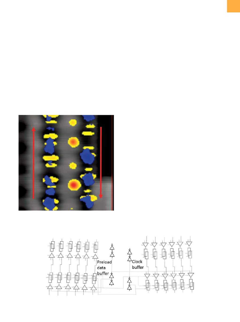
laser scanning area. Figure 2 is an example of an LVI image,
showing the data and clock signals. Because LVI collects
data in the frequency domain, it is necessary to map the
transistor switching at a particular frequency. It is conve-
nient to run the clock and data at different frequencies so
that both the clock and data paths in the scan chain can
be individually and simultaneously traced. Thus, it quickly
became apowerful fault isolation technique for scan chain
failures. With subsequent LVP, the defect for a scan chain
failure can be narrowed down to an inverter or a node.
IN-LINE SCAN CHAIN LOGIC MACRO
DESCRIPTION
The in-line scan chain logic macro can first be tested
at metal-4 layer for early yield learning. It is comprised
of several scan chains organized in 16 blocks. Each block
has six packs, and each pack has six scan chains, which
share the same clock buffer and preload data buffer (Fig.
3). Each scan chain group/block is composed of a differ-
ent type of level-sensitive scan design and general scan
Fig. 2
Example of LVI image for a scan chain: blue for data
signal, yellowfor clock signal, and redarrows for data
propagation direction
Fig. 3
Diagram of scan chains in a pack showing the latches at the same position for six scan chains in a pack that share the
same preload data buffer and clock buffer