


 4 / 66

edfas.org
ELECTRONIC DEVICE FAILURE ANALYSIS | VOLUME 18 NO. 4
4
EDFAAO (2016) 4:4-14
1537-0755/$19.00 ©ASM International
®
LVI AND LVP APPLICATIONS IN IN-LINE SCAN CHAIN
FAILURE ANALYSIS
Zhigang Song and Laura Safran, Globalfoundries
zhigang.song@globalfoundries.comL
aser voltage imaging (LVI) has the unique capability
of mapping the periodic signal in a device under
test (DUT). It is very suitable for scan chain diagno-
sis because data propagation through the scan chain is
clocked with a periodic signal. Thus, LVI can easily iden-
tify the broken point for a scan chain failure, whether its
defect is in the data pathor in the clock path. Laser voltage
probing (LVP) involves acquiring the waveform in a time
domain froma particular point, such as the signal broken
point identified by LVI, and a reference point. This can
further confirm the failure and help with understanding
the failure signature. This article discusses combining
these two techniques in an in-line scan chain logic macro
diagnosis, which has greatly improved the failure analysis
success rate.
INTRODUCTION
Historically, static random access memory (SRAM)
yields have been the only qualification metrics during
technologydevelopment, and consequently, failure analy-
sis of SRAM is themain feedback for process improvement
and yield learning.
[1,2]
This is because the high density and
small feature size of SRAMmake its yield very sensitive to
process variation, and the failing bit cells can be precisely
localized for physical failure analysis. As microelectronic
technology progresses in the nanometer realm, logic
circuits and structures are also becoming dense and
sensitive to process variation. Logic failures may also
have root causes different from SRAM failure. If these
technology weak points for logic circuits are not detected
and resolved during the technology development stage,
they will greatly affect the product manufacturing yield
ramp, leading to longer design time tomarket. Moreover,
analysis of logic failure in the product is much more dif-
ficult and time-consuming, involving tester-based fault
isolation
[3,4]
and software-based scandiagnosis.
[5,6]
Thus, it
is very important to have an in-line scan chain logicmacro
implemented for early detection of the logic circuit weak
points during technology development. Furthermore,
LVI’s unique capability to map the periodic signal
[7-9]
in
a DUT makes it a great diagnostic technique for scan
chain failure, whether the scan chain failure is due to a
clock issue or an issue with the latch itself. In addition,
LVP probing
[10-13]
can further confirm the failure identi-
fied by LVI. The combination of LVI and LVP application in
scan chain diagnosis has improved the in-line scan chain
logic failure analysis success rate to that of SRAM failure
analysis. This article reviews the LVI and LVP technique
principles and their unique capabilities, then describes
an in-line scan chain logic macro, and finally presents
three case studies of LVI and LVP applications in in-line
scan chain failure analysis.
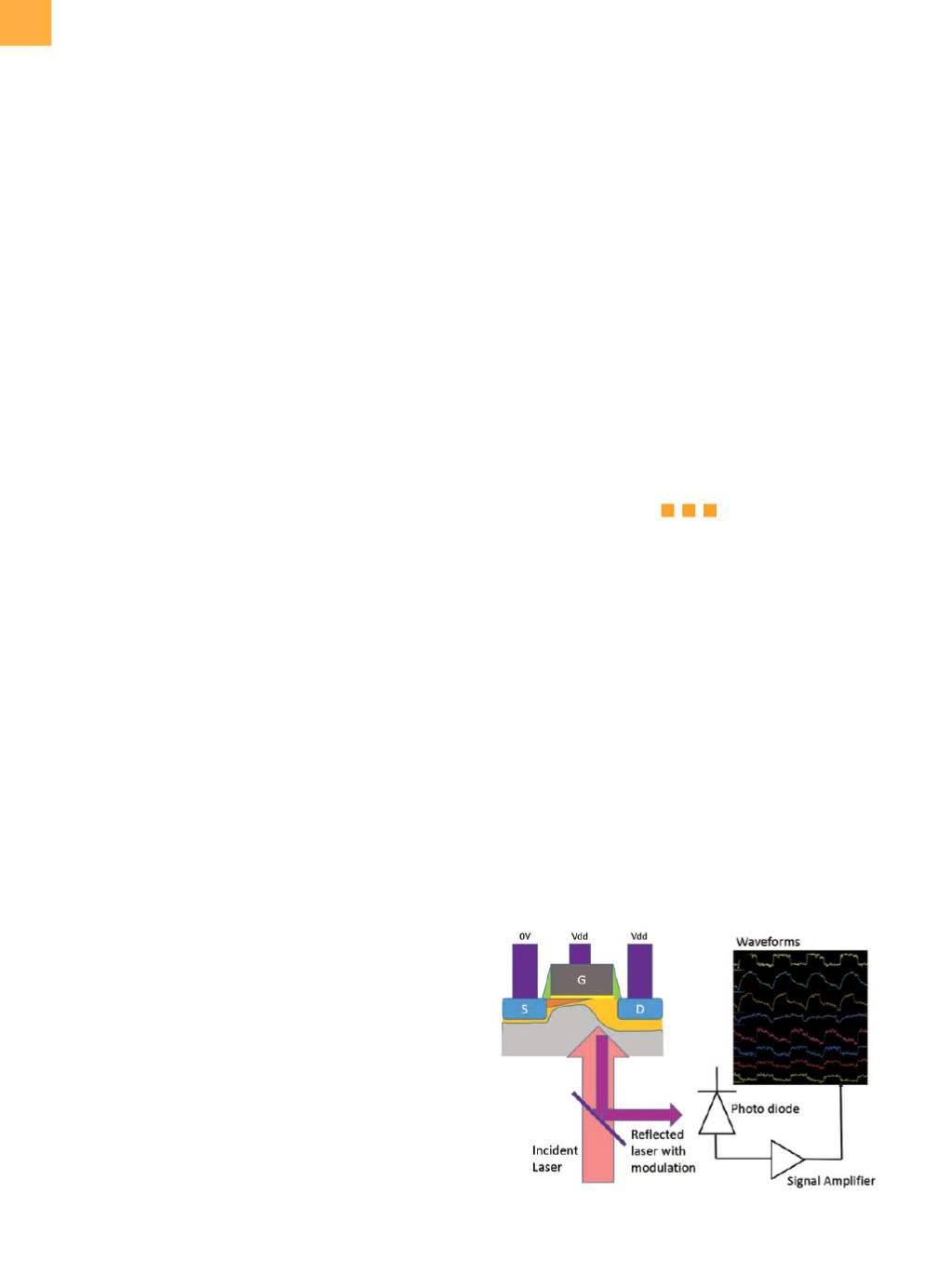
LVI AND LVP TECHNIQUE REVIEW
Laser voltage probing
[10-13]
employs a near-infrared
laser beam shining on the transistor active area through
“THE COMBINATION OF LVI AND LVP
APPLICATION IN SCAN CHAIN DIAGNOSIS
HAS IMPROVED THE IN-LINE SCAN CHAIN
LOGIC FAILURE ANALYSIS SUCCESS RATE
TO THAT OF SRAM FAILURE ANALYSIS. ”
Fig. 1
LVP schematic