


 8 / 66

edfas.org
ELECTRONIC DEVICE FAILURE ANALYSIS | VOLUME 18 NO. 4
8
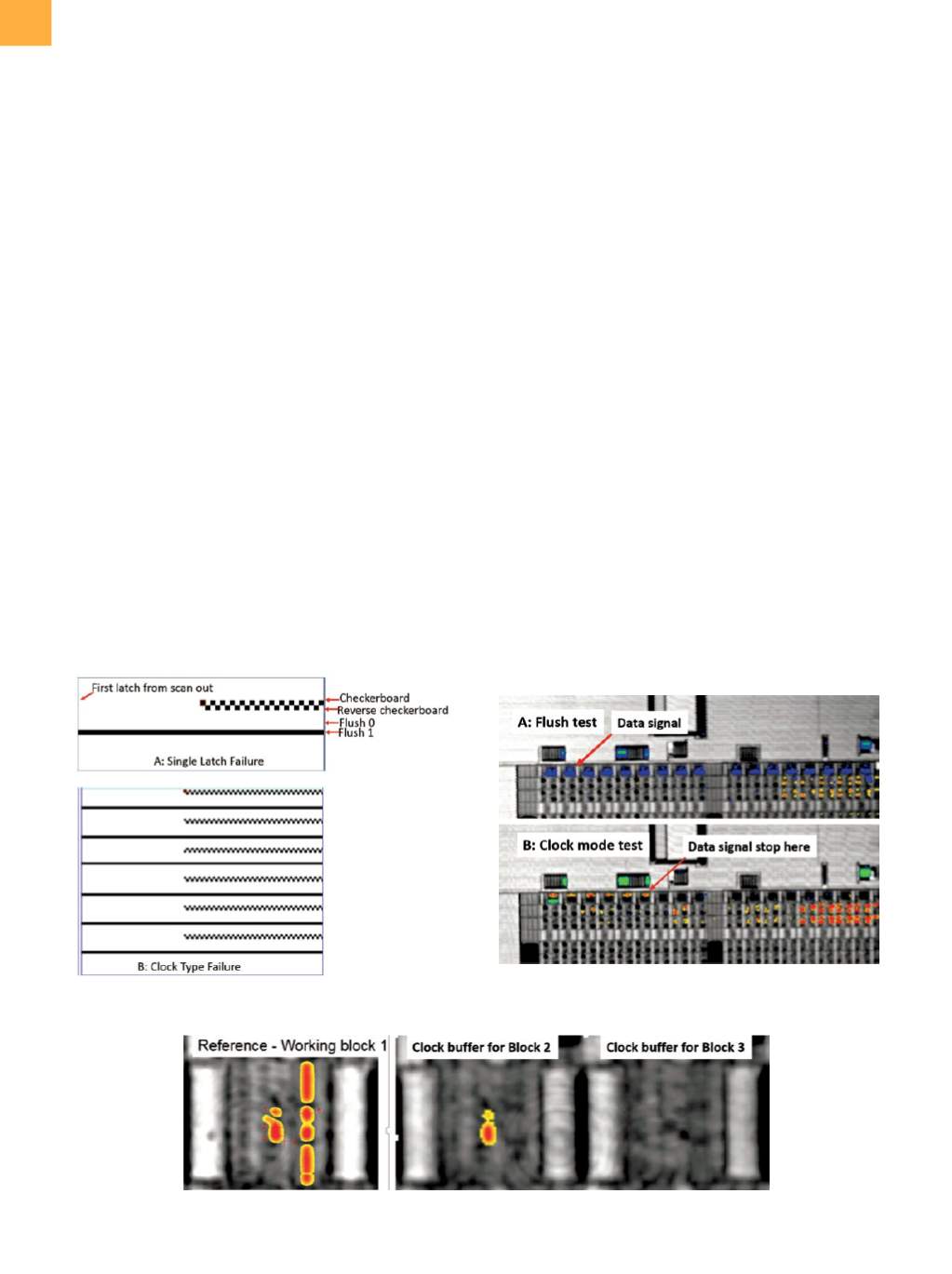
checkerboard row, pinpoints the latch callout (Fig. 5a).
In Fig. 5(b), the six scan chains in a pack are failing at the
same latch position, indicating a clock-type failure.
CASE STUDIES
Because the in-line scan chain logicmacro is diagnos-
able and single-latch fallout canbe identifiedbasedon the
preload test, ahard single-latch failuremaybe successfully
analyzedwith routine physical failure analysis (PFA) using
top-down scanning electron microscopy (SEM) inspec-
tion. However, as defined previously, the root cause of a
clock-type failure could be any failure in the buffers and
the interconnects of the preload data and clock lines, or a
bridging fault in the preload data and clock input circuits
inany individual latches. This involves a large area. Clearly,
it is more challenging to perform PFA on a clock-type
failure. Thus, for clock-type failures, LVI and LVPdiagnoses
are necessary for localizing the failure to a small area prior
to PFA. In addition, for soft single-latch failures, although
the possible defective area is the same as for hard single-
latch failures, the defect causing a soft single-latch failure
ismuch smaller andmore subtle. Due to the subtle nature
of the defect and the large number of transistors (asmany
as 50 per latch) that must be inspected, the success rate
with routine PFA for soft single-latch failures is very low.
With the help of LVI and LVP, the success rate has been
improved to approximately 85%. This section describes
three cases that demonstrate how to apply LVI and LVP in
diagnosing scan chain clock-type failures and soft single-
latch failures. The root causes of these failureswere found
by subsequent PFA.
SKIP TEST SCAN CHAIN FAILURE
As previously mentioned, the in-line scan chain logic
macrohas beendivided into 16 blocks, withdifferent latch
types or layout variations in each block. A skip test scan
chain is implemented to enable each block to be tested
individually. Before testing the 16 blocks of main scan
chains, a skip test is performed to check the integrity of the
skip test scan chain. In the first case study, a chip suffered
fromskip test failure. First, LVI was performedwith the skip
test scan chain under flush test, and the LVI image showed
that the data could pass through the skip test scan chain
successfully (Fig. 6a). However, the data signal stopped
at the sixth latch, aligning with the last pack of block 1,
when the skip test scan chain was run under clock mode
test (Fig. 6b). This implied that the skip test scan chain
failure was due to a clock signal issue. Both L clock and D
clock signals weremappedwith LVI, and it was found that
the L clock signal propagation was fine, while the D clock
Fig. 5
Examplesof (a) single-latchand (b) clock-type failures
Fig. 6
LVI image for the skip test scan chain. (a) Flush test.
(b) Clock mode test
Fig. 7
LVI images at the clock buffers (D clock) for block 1 (reference), block 2, and block 3
(continued on page 10)
LVI AND LVP APPLICATIONS IN IN-LINE SCAN CHAIN FAILURE ANALYSIS
(continued from page 6)