


 18 / 66

edfas.org
ELECTRONIC DEVICE FAILURE ANALYSIS | VOLUME 18 NO. 4
18
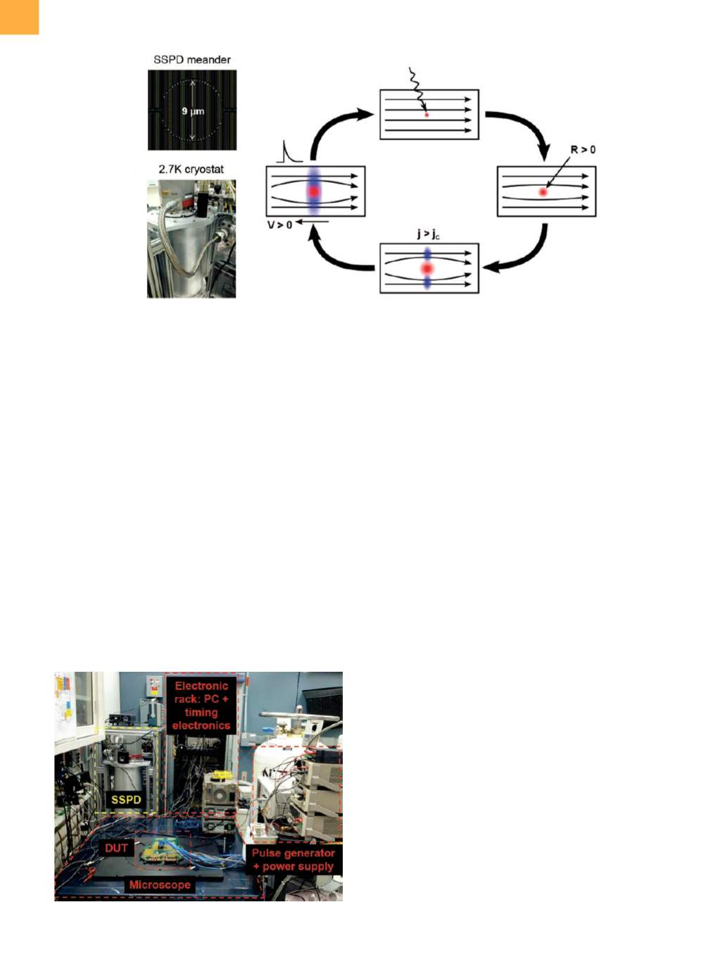
Fig. 3a) that is kept below the superconducting criti-
cal temperature of a few degrees Kelvin by using a
closed‑cycle cryostat (Fig. 3b). The detector is biased at
a constant current. When a photon hits the meander, it
creates a hot spot (Fig. 3c, top) that makes the current
crowd toward the remaining portion of the nanowire
(Fig. 3c, right), causing it to exceed the critical current
density value,
j
c
(Fig. 3c, bottom). At this point, the
meander superconductivity is broken (i.e., it becomes
resistive), and a voltage pulse across the SSPD (Fig. 3c, left)
can be detected by the front‑end electronics. After a few
nanoseconds, the meander returns to superconductivity
and is ready to detect a new incoming photon.
LOW-VOLTAGE SENSITIVITY
The typical experimental setup used to acquire TRE
waveforms with the SSPD is shown in Fig. 4. A pulse gen-
erator provides a clock to the DUT while its spontaneous
emission is collected by the high-NA solid immersion lens
of amicroscope and, through a single-mode fiber, is fed to
the SSPD. The delay between each detected photon from
theSSPDand the clock synchronization signal ismeasured
by the timing electronics. The cumulative histogramof all
the photon arrival times is used to reconstruct the TRE
waveform. Note that most of the optical tools (e.g., those
from FEI and Hamamatsu) can be retrofitted to perform
TRE measurements. The only requirements are a fiber
port to connect the SSPD as well as timing electronics to
reconstruct the measured waveform.
Figure 5 shows the emission intensity measured at
different chip supply voltages from an inverter gate in
32 nm silicon-on-insulator (SOI) technology using two
generations of SSPD.
[10]
The switching emission signal
is measured as the amplitude of the switching emission
peak in the TREwaveform, while the noise is the standard
deviation of the intensity level correspondent to the
semiperiod during which the field-effect transistor (FET)
is conductive. Figure 5 shows that themeasurement noise
is limited by the detector noise (dark-count rate, or DCR)
for voltages lower than 0.65 V. The second-generation
SSPD is characterized by a higher system detection effi-
ciency; as a consequence, both the switching emission
Fig. 3
(a) NbNmeander, shaped in a 9-µm-diameter circle, that was used for this work.
[10]
(b) Three-stage closed‑cycle cryostat
that houses the SSPD.
[10]
(c) Working principle of the SSPD. The detector is biased at a constant current lower than the
critical current. When a photon hits the nanowire, a hotspot is created. The current crowds at the edges, and when it
becomes higher than the critical current value, the superconductivity is lost, leading to a voltage pulse that can be
detected by external electronics.
(a)
(b)
(c)
Fig. 4
Experimental setup used to acquire TRE waveforms