


 17 / 58

 edfas.org
1 7
ELECTRONIC DEVICE FAILURE ANALYSIS | VOLUME 18 NO. 2
Soft errors are a dominant reliability concern for
advanced silicon process technologies because the asso-
ciated failure rates are constant with time and therefore
can be present over thewhole operational life of a circuit.
Furthermore, with technology progression, the rate of
failure of circuits or systems tends to increase as ever-
higher densities of transistors are incorporated to improve
performance, cost, and functionality. With the introduc-
tion of the FinFET, it is important to understand how soft
errors are impacted and what, if any, new soft-error-rate
(SER) issuesmay be introducedby this change. This article
reviews recent work aimed at characterizing soft-error
effects in SRAMcircuits fabricatedwith bulk silicon FinFET
transistors. Experimentally determined error rates are
combinedwith technology computer-aideddesign (TCAD)
simulations toprovide a clear understanding of the charge
generation and collection processes that occur in both
planar and FinFET transistors. As shown, the introduction
of the FinFET leads to a significant improvement in SERs
because of a large reduction in charge collection resulting
from the more limited geometry of the fin compared to
the planar structure.
EXPERIMENTAL DETAILS
All accelerated tests were conducted following the
JEDEC JESD89 testing standard.
[11]
SRAM circuits with a
range of manufacturing processes and bit-cell sizes were
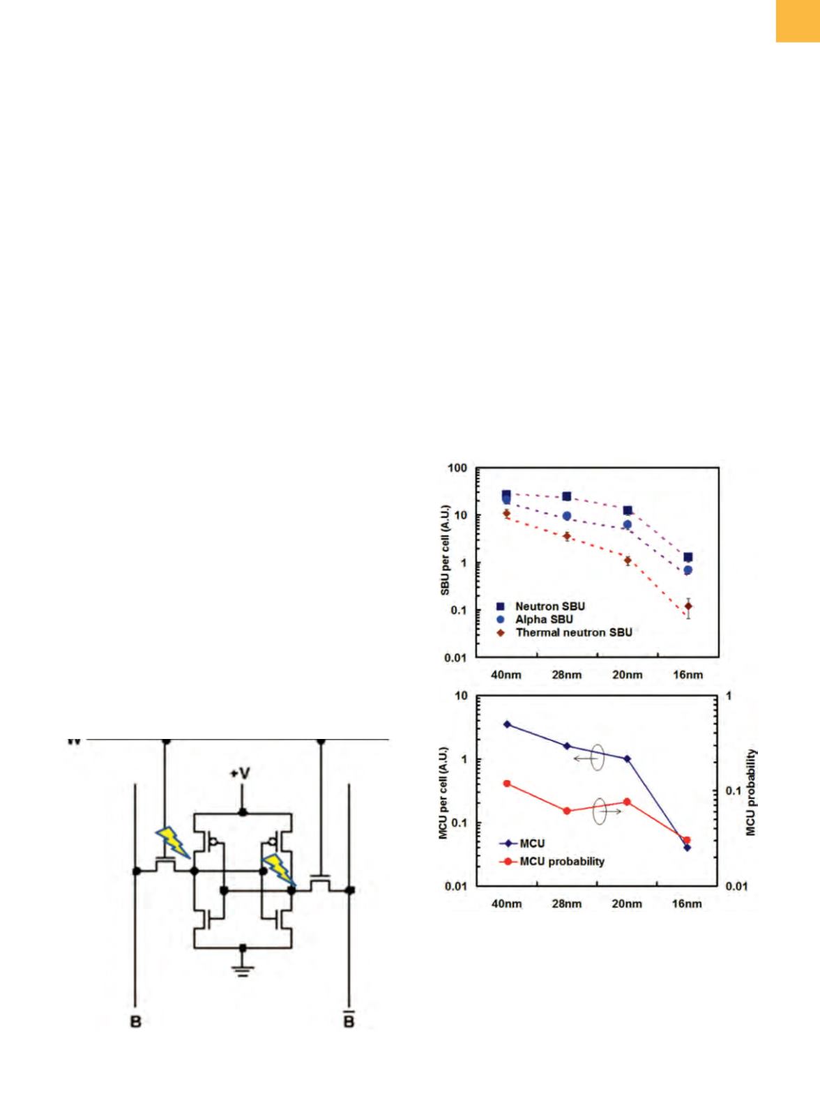
tested. The SRAM devices used the standard 6-transistor
(6T) cell design, as shown in Fig. 2. High-energy neutron
characterization of 6T-SRAMs was carried out using neu-
trons with an atmospheric-like energy spectrum, where
the energy range is up to 150 MeV.
[12]
Neutrons were
incident normal to the surface of the SRAMs. The fluence
(neutron beam flux
×
exposure time) of each test run
was ~1
×
10
9
neutrons/cm
2
. Thermal neutron SER tests
were conducted at the Laboratoire
Léon Brillouin facil-
ity in France using a low-energy neutron source with a
25-meV-equivalent neutron spectrum.
[13]
Alpha SER tests
wereperformedusinganAm-241 irradiation sourceplaced
on the packaging-decapped SRAM chip. The gap between
the irradiation source and the tested chip surface was
~1mm inall cases. Testswere performeddynamicallywith
a clock cycle of 100 ns. Testswere performed at roomtem-
perature using a checkerboard all-0 or all-1 test pattern.
Experimental data are presented as the average of all test
patterns. Neutron errors were normalized to the neutron
flux at the sea level of New York City, that is, 13 counts/
cm
2
/h for high-energy neutrons and 6.5 counts/cm
2
/h for
thermal neutrons. Alpha particle errors were normalized
to an emission rate of 0.001 count/cm
2
/h.
SINGLE-BIT ERRORS IN SRAM CIRCUITS
Figure 3 shows the experimentally determined trend
of single-bit upsets (SBUs) for SRAM circuits as a function
Fig. 2
6T-SRAM cell
Fig. 3
(a) Measured alpha, thermal neutron, and high-energy
neutronSBUevents for 40, 28, and 20 nmplanar SRAMs
as well as a 16 nm FinFET SRAMwith nominal voltage.
Dashed lines are modeled results using Eq 1 for all
irradiation sources. (b) High-energy-neutron-induced
multicell upset (MCU) events and MCU probability
of SRAMs (MCU per total upsets) as a function of
technology
(a)
(b)