


 18 / 58

 edfas.org
ELECTRONIC DEVICE FAILURE ANALYSIS | VOLUME 18 NO. 2
18
of technology progression for recent silicon technology
nodes. Note that the FinFET transistor was introduced at
the 16 nmnode. The error rate has trended down over this
technology range for all the upset mechanisms. However,
the introduction of the FinFET has led to a large decrease
in the magnitude of errors (approximately a factor of 10)
compared to what would be expected from an extrapola-
tion of the data for planar transistors.
Themagnitude of errors for planar transistors is readily
calculated using the following expression:
S
=
FA
s
exp(−
Q
coll
/
Q
crit
)
(Eq 1)
where
F
is the flux of particles incident on the silicon
surface, and
A
s
is the sensitive area for charge collection.
The relation indicates that
S
decreases with lowering
Q
coll
when
Q
crit
of the device is constant. The exponential
function exp(−
Q
coll
/
Q
crit
) is the probability of an error occur-
ring, which depends on the nature of energetic particle
involved. The downward trend of
S
occurs because the
sensitive area,
A
s
, has decreased faster than the decrease
in the critical charge with technology scaling. Shown in
Fig. 3 are relative failure rates calculated using Eq 1. The
large reduction of
S
with the introduction of the FinFET
is beyond what is expected on the basis of changes in
A
s
alone and implies that the probability of an error is
reduced. This must involve modification of the collected
charge with the FinFET geometry.
Charge collection resulting from the impact of an
energetic particle with the silicon substrate occurs by
two mechanisms:
• Charge drift in the drain region when the ion track
crosses the drain directly
• Charge diffusion via the
p
-
n
junction to the drain region
when the ion track does not cross the drain
In planar devices, charges associated with the ion
tracks penetrating the silicon substrate are deposited in
the drain directly and also under the drain region, which
then diffuse to the drain. While the fin body of the bulk
FinFET is connected to the substrate, the volume of silicon
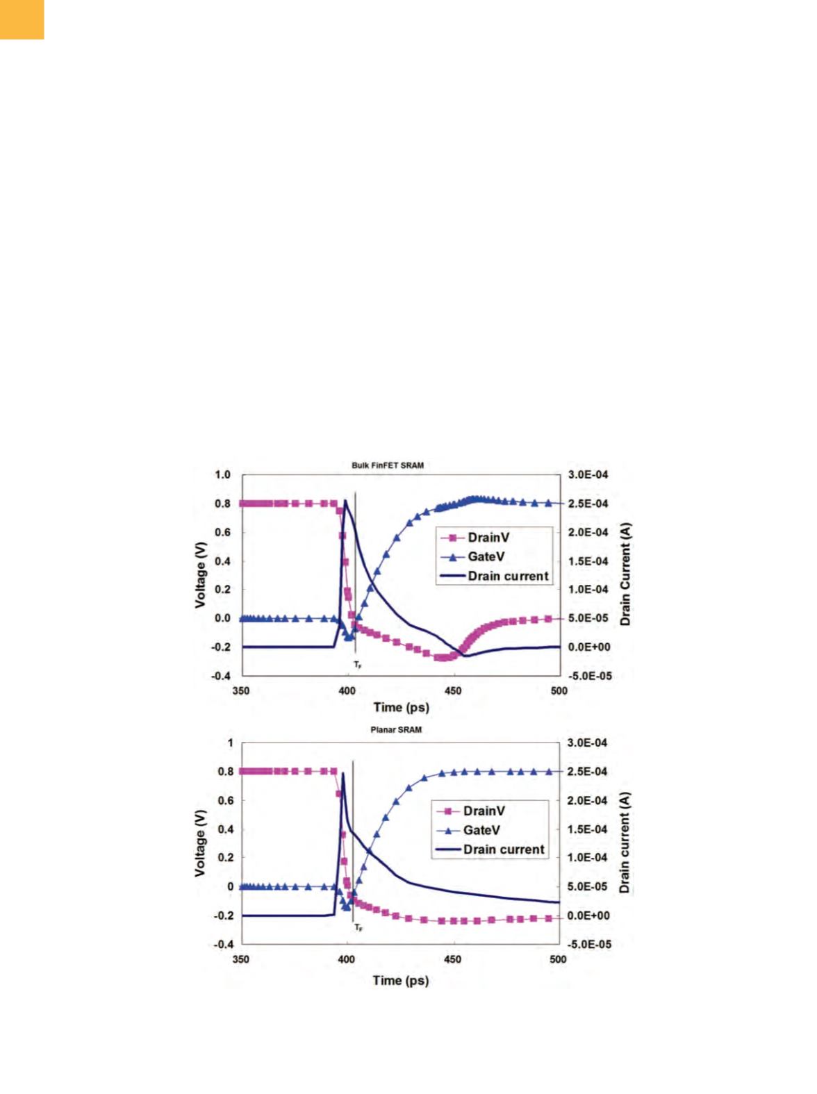
(a)
(b)
Fig. 4
Gate voltage and drain voltage change as well as drain current variation when a heavy ion crosses the drain horizontally
in (a) bulk FinFET SRAM and (b) planar SRAM. Data-flipping time,
T
F
, is the time where the increasing gate voltage crosses
the falling drain voltage.