


 20 / 58

 edfas.org
ELECTRONIC DEVICE FAILURE ANALYSIS | VOLUME 18 NO. 2
20
both devices are consistent in the first stage of charge col-
lection, which is dominated by drift. In the second stage,
the drain current of the planar SRAM is higher than that
of the FinFET SRAM. This is because of additional charge
diffusion from the substrate. In contrast, the charge in the
FinFET SRAM is collected almost entirely by drift because
the ion track only crosses the drain of the fin body. For
the planar SRAM, the ion track crosses not only the
planar drain but also the substrate. The
Q
coll
is obtained
by integrating the current up to 1000 ps, which is 4.71 fC
for the FinFET SRAM and 7.92 fC for the planar SRAM. The
comparison of
Q
coll
of the FinFET and planar SRAMs with
ion strikes with different LETs is shown in Fig. 5(b). On
average, when the ion track crosses the drain horizontally
along the drain body,
Q
coll
of the FinFET SRAM is ~0.6
×
smaller than that of the planar SRAM up to an LET of
15 MeV, which is the range of charge deposition of terres-
trial neutron-induced ions in silicon.
[10]
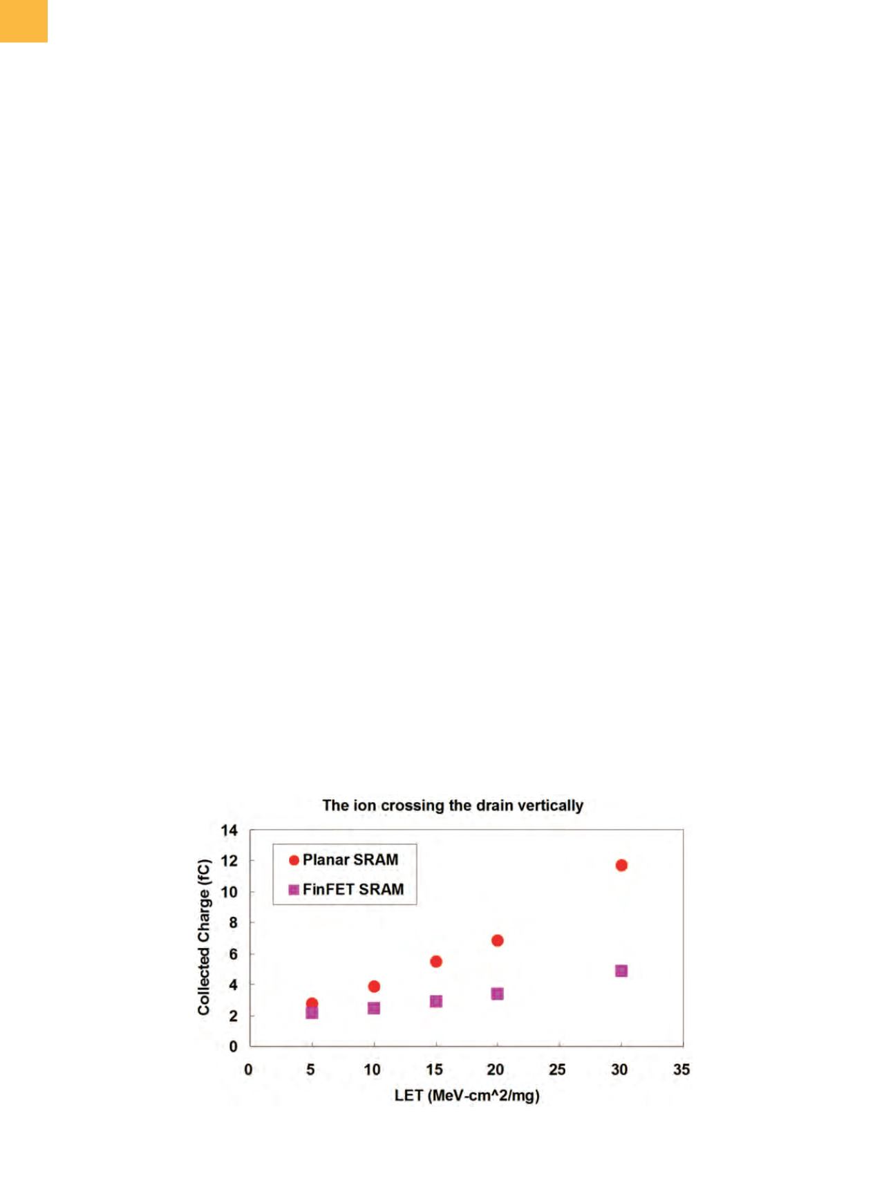
Figure 6 compares
the FinFET
Q
coll
and planar SRAMs when the incident ion
track crosses the drain vertically fromthe top. In this case,
Q
coll
of both FinFET and planar SRAMs increases compared
to the ion crossing horizontally, because charge diffu-
sion from the substrate increases when the ion track is
at normal incidence to both the drain and the substrate
under the drain. The averaged
Q
coll
of the FinFET SRAM for
LETs up to 15 MeV is close to a factor of 0.6 that of planar
SRAM in the normal incidence case.
When the ion track does not cross the drain, deposited
charges are collectedby diffusion only. The planar SRAM is
sensitive to the diffused charges generatedby the ionpen-
etrating under the drain because there is a wide sensitive
volume of charge collection. Figure 7(a) shows the varia-
tion of the drain voltage of the planar SRAMwith different
LETs. The drain voltage drops with time when the LET of
the ion is over 5MeV. In the bulk FinFET, only the finbody is
connectedwith the substrate. For the same ion strike, the
ionmust depositmore charge in the substrate to cause the
bulk FinFET SRAM to flip comparedwith the planar SRAM.
The increasing LET required to cause a bit flip is shown in
Fig. 7(b). The drain voltage of the bulk FinFET SRAM does
not flip until the LET is 60 MeV. In the terrestrial environ-
ment, themaximumenergy of incident neutrons is limited
to 1 GeV.
[15]
The maximum energy deposition (or LET) of
a neutron-induced ion in silicon is 15 MeV. Therefore, the
planar SRAM flips easily in the 15 MeV range of LET. The
bulk FinFET SRAM is immune to an upset in this energy
range. That is,
Q
coll
of terrestrial neutron-induced energetic
ions from the silicon substrate is ineffective in causing a
change in the data stored in the SRAM bit cell.
It has been shown that the maximum probability
of neutron-induced ions crossing the drain is 0.25 (i.e.,
the probability of ions not crossing the drain is 0.75) for
a fixed-drain area of a planar device.
[15]
In the situation
studied here, where the overall geometries of the FinFET
and the planar SRAMs are the same, when the ion crosses
the drain,
Q
coll
of the bulk FinFET SRAM is only 0.6 that of
the planar SRAM. Without the ion crossing the drain, the
FinFET SRAM is immune to upsets in the terrestrial envi-
ronment. Therefore, for awide range of incident ions,
Q
coll
of a FinFET SRAM should be 0.6
×
0.25 = 0.15 compared
with a planar SRAM. Using the
Q
crit
determined in the
previous section and the top drain area of the FinFET of
0.4 that of the planar device, the relative SER of the bulk
FinFET SRAM is estimated to be ~0.06 compared with the
planar SRAM; that is, it is anticipated that FinFETs will
Fig. 6
Q
coll
of planar and FinFET SRAMs from the normal incident track crossing the drain with different LETs