


 25 / 58

 edfas.org
25
ELECTRONIC DEVICE FAILURE ANALYSIS | VOLUME 18 NO. 2
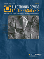
Fig. 14
Comparison for drain transient currents of 40, 28, and 20 nm planar
n
-FETs as well as a 16 nm
n
-FinFET with an identical
relative
D
x
of 0.45
MCU probabilities between technology nodes were
obtained by assuming all ion strikes incident to the region
of the 40 nm
n
-FET drain result in a data error; that is,
the probability of upsets at
D
x
= 0 of the 40 nm SRAM is
1. Then all
Q
coll
(
D
x
) are normalized to
Q
coll
(0) of the 40 nm
to give the probability
P
MCU
(
Q
crit
,
Q
coll,
D
x
). Figure 13 shows
that the calculated relative upset probability compares
well to that determined from the measured MCU cluster
distributions. It canbe clearly observed in Fig. 13 that MCU
probability at a given cluster length decreases with tech-
nology scaling, as is evident by the increasingly negative
slope of the MCU cluster length distribution; this implies
that factors in addition to the geometry of the bit cell
impact MCU probability. Figure 14 compares simulated
transient currentswith the identical relative strike location
(
D
x
= 0.45) for all devices. For
D
x
= 0.45, all deposited charge
is collected by diffusion only. With the identical relative
D
x
, the diffused current peak decreases with scaling. The
authors suggest this suppression occurs due to the reduc-
tion of chargemobility caused by increasing doping levels
of the substrate beneath the transistor, because this is the
primary region where diffusion of the charge occurs.
[17,18]
The transport of charge in semiconductors is dominat-
ed by scattering by the ionized impurities in doped silicon.
In TCAD simulations, the charge mobility dependence on
substrate doping is accounted for by using the Masetti
model,
[19]
which models charge mobility in arsenic-,
phosphorus-, and boron-doped silicon over a wide
range of carrier concentrations (10
13
to 10
21
cm
−3
). Higher
doping concentration in the silicon leads to lower charge
mobility due to ionized impurity scattering. To determine
the substrate doping impact on
Q
coll
, the authors re-ran
the TCAD simulations but intentionally turned off the
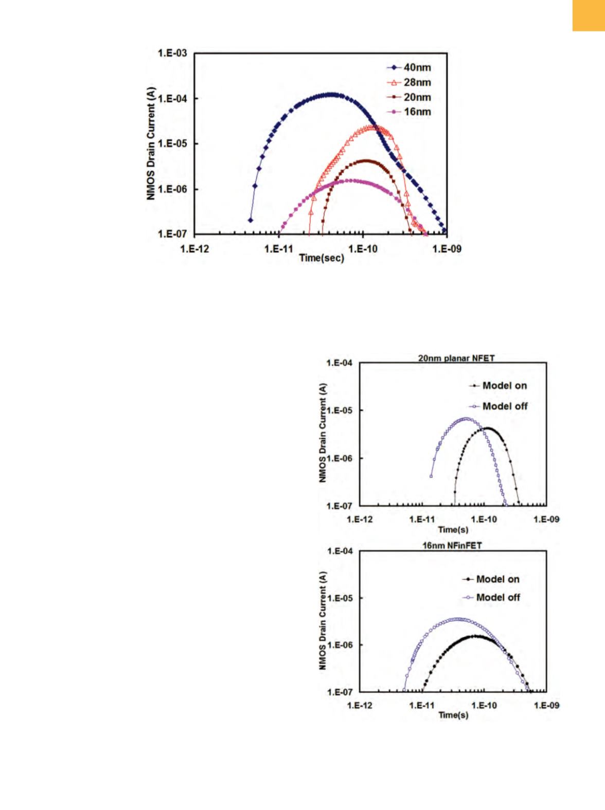
Fig. 15
Comparison for transient currents of (a) 20 nm
n
-FET
and (b) 16 nm
n
-FinFET with strike locations at the
relative
D
x
= 0.45 before and after turning off the
doping-dependent charge mobility model
doping-dependent mobility degradation model. Figure
15 shows the comparison for transient diffusion currents
only of the 20 nm planar FET and the 16 nm FinFET with
(a)
(b)