


 23 / 58

 edfas.org
23
ELECTRONIC DEVICE FAILURE ANALYSIS | VOLUME 18 NO. 2
causes error is charge sharing, which results from diffu-
sion of charge to cells that are adjacent to the cell directly
involved in the particle strike. The authors recently have
shown that the primary mechanism responsible for MCU
events in both planar transistors and FinFETs is charge
sharing, so bipolar amplification is not considered further
in this discussion. A charge-sharingmechanism is primar-
ily characterized by a decrease in the probability of MCU
events with increasing physical distance over which the
MCU event occurs.
To understand the origin of MCU events in SRAM
devices, the authors performed charge-collection simula-
tions using Synopsys’ Sentaurus TCAD. Details are given
in Ref 16. A heavy ion with LET of 150 fC/µm was nor-
mally incident at different locations in the vicinity of the
n
-FET drain, as shown in Fig. 9. The strike location
D
x
= 0
indicates the heavy ion is normally incident to the
n
-FET
drain region, whereas the relative
D
x
> 0 means the ion
is normally incident to the silicon surface with a relative
distance away from the edge of the
n
-FET drain along the
D
x
direction. The distance unit of all devices is the same as
the unit of MCU cluster length shown in Fig. 10.
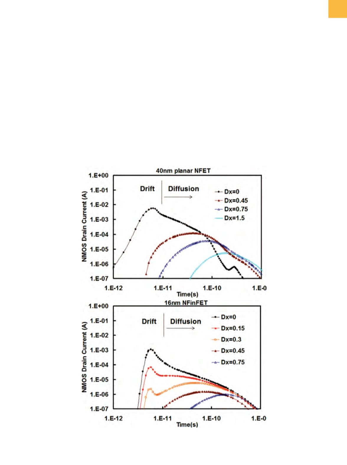
Figure 11 shows the transient currents of the 40 nm
planar
n
-FET and the 16 nm
n
-FinFET as a function of the
strike location. The current consists of an initial spike
due to the drift component, followed by a tail at larger
times from the diffusion component. The drift current is
collectedwhen the ionpenetrates through thedraindeple-
tion layer, whereas the diffusion current is collected from
the substrate via the drain
p-n
junction. When the strike
occurs outside the drain, the drift component disappears,
leaving only the diffusion current. The drift currents of the
Fig. 11
Drain transient currents of (a) 40 nmplanar
n
-FET and (b) 16 nm
n
-FinFET with different strike locations. The ion strike with
an LET of 150 fC/µm starts at 4
×
10
−12
s.
(a)
(b)