


 9 / 62

 edfas.org
9
ELECTRONIC DEVICE FAILURE ANALYSIS | VOLUME 18 NO. 1
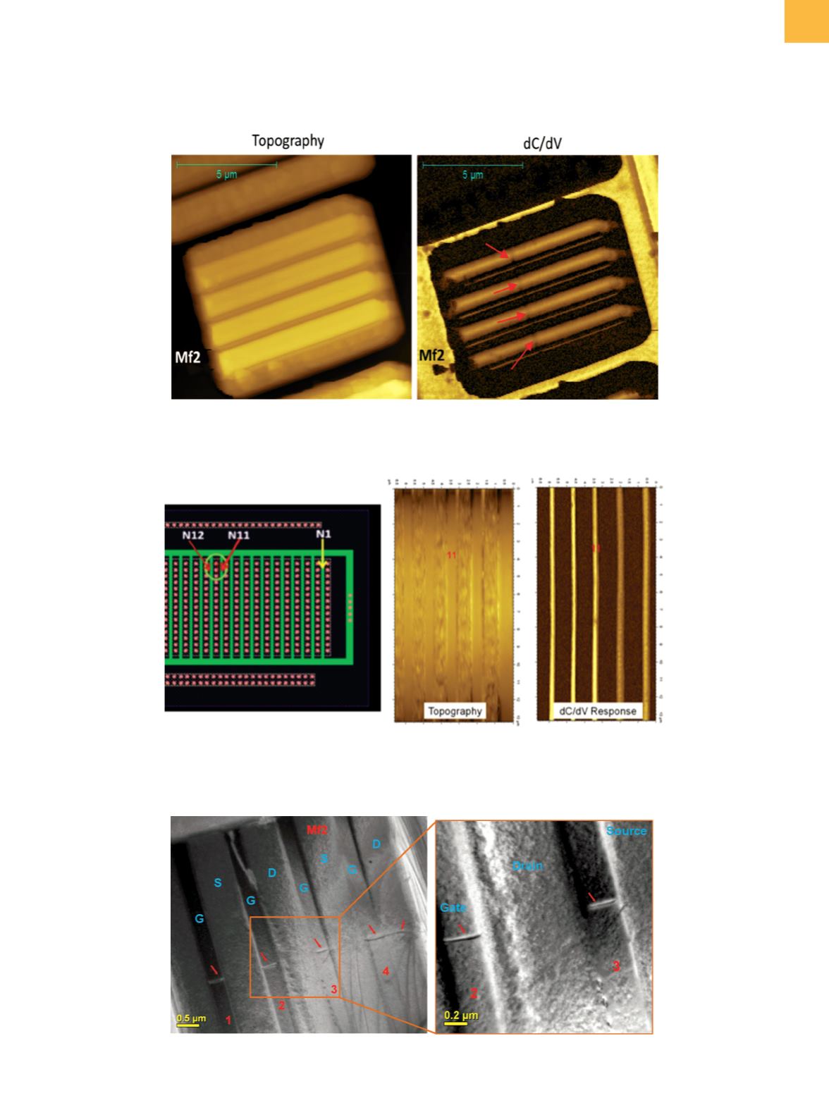
Fig. 7
AFM/SMM characterization of “pipeline” silicon defect impacting two neighbor transistors and crossing the full active area
in a part from case 2. No conclusive anomaly is visible in the topography image; however, the dark line is indicated with
red arrows in the dC/dV response image.
Fig. 8
AFM/SMM characterization of silicon dislocation crossing the full active area in case 3. (a) Localization of failure in device.
(b) AFM and SMM characterization. No anomaly in the topography or dC/dV response images
(a)
(b)
Fig. 9
TEM images of pipeline defect fingers for case 2
(several microns long) in the active area, perpendicular
to the source-drain fingers (Fig. 10). In case 3, it is sus-
pected to be a dislocation. By comparing TEM signatures
of pipeline and silicon dislocations, it was not possible to
make an obvious distinction between these two different
signatures by TEM analysis alone. However, TEM analysis