


 10 / 62

 edfas.org
ELECTRONIC DEVICE FAILURE ANALYSIS | VOLUME 18 NO. 1
10
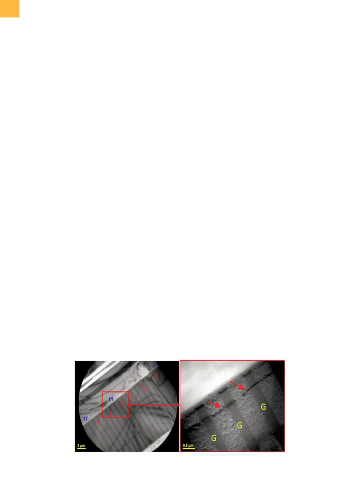
Fig. 10
TEM images of dislocation in silicon in case 3. The gates are indicated by the letter “G.”
is useful in determining the real size and shape of the
physical defect in silicon.
[10]
DISCUSSION: PIPELINE OR
DISLOCATION
PIPELINE AND DISLOCATION PHYSICAL
DISTINCTIONS
The complementary electrical and physical analyses
performed in this work demonstrated that the defects
can be imaged, but their natural differentiation is more
difficult to identify:
• There is no distinction possible in terms of electrical
failure (similar failuremode, current leakage level, etc.).
• There is no distinction of TLS or EMMI signature (spot
signature, sensitivity, etc.).
However, basedonmultiple case studies, the following
approaches could be used to distinguish pipeline defects
and dislocations. First, PVC at the silicon level using
SEM can highlight pipeline defects. Based on the physi-
cal behavior of a free carrier introduced by phosphorus
implanted in the channel, it is possible to generate PVC at
the pipeline. As a result, the SEM electron beam formed a
picture with a contrast variation in the defective area. It is
believed that this phenomenon is either not possible on a
dislocation, or the dopant concentration in the dislocation
core is not sufficient to produce PVC in the SEM, allowing
their natural differentiation. In addition, another concern
is the depth of the defect; it is commonly accepted that
dislocations are found in subsurface regions compared
to pipelines, which are normally located at the surface of
the channel. Therefore, PVC is more effective in localizing
pipeline defects.
Crystal delineation etching usingWright etch solution
is an interesting complementary analysis to PVC in the
SEM. Typically, the pipeline defect appears as a three-
dimensional bump (relief) in the channel, whereas the
dislocation creates an overetched line area, as a cavity
(Fig. 11). While this method offers another way to differ-
entiate pipeline and dislocations, this approach suffers
from the following limitations:
• If the defect is located a few nanometers from the
surface of the active area, etching can consume the
defect.
• If the defect is located in the substrate volume, it
could be difficult to define the correct etching time to
expose it.
Furthermore, the problems of reproducibility in the
etchingprocess caneasilydestroy thedefect. Alternatively,
nondestructive dopant profiling techniques (SMMor scan-
ning capacitance microscopy, or SCM) can be used on a
single defective unit to improve analysis success. The
surface-level capacitance change due to a pipeline defect
is activated by phosphorus atoms (
n
-type) by creating an
inversion line in the channel; it produces a line contrast in
the dC/dV response image. However, it was demonstrated
that the dislocation did not produce such dC/dV contrast,
possibly because of the depth location of the dislocation
or a too-low concentration of active dopant. This point
was not studied in this work and is considered a prospect
for future work.
Planar TEM analysis offers the best solution for
determining the size and shape of both pipeline and
dislocation defects. Unfortunately, it is not easy to dis-
tinguish between pipeline and dislocation because of
similar physical signatures on TEM images. Advanced
transmission electron microscopes equipped with high-
spatial-resolution electron energy-loss spectrometry
capability may be an option for detecting phosphorus
atoms in the pipeline.
Based on themultiple experiments presented, ameth-
odology for analyzing those failures is proposed:
• When several parts are available:
The best practice
should be to first perform Wright etch delineation