


 15 / 62

 edfas.org
15
ELECTRONIC DEVICE FAILURE ANALYSIS | VOLUME 18 NO. 1
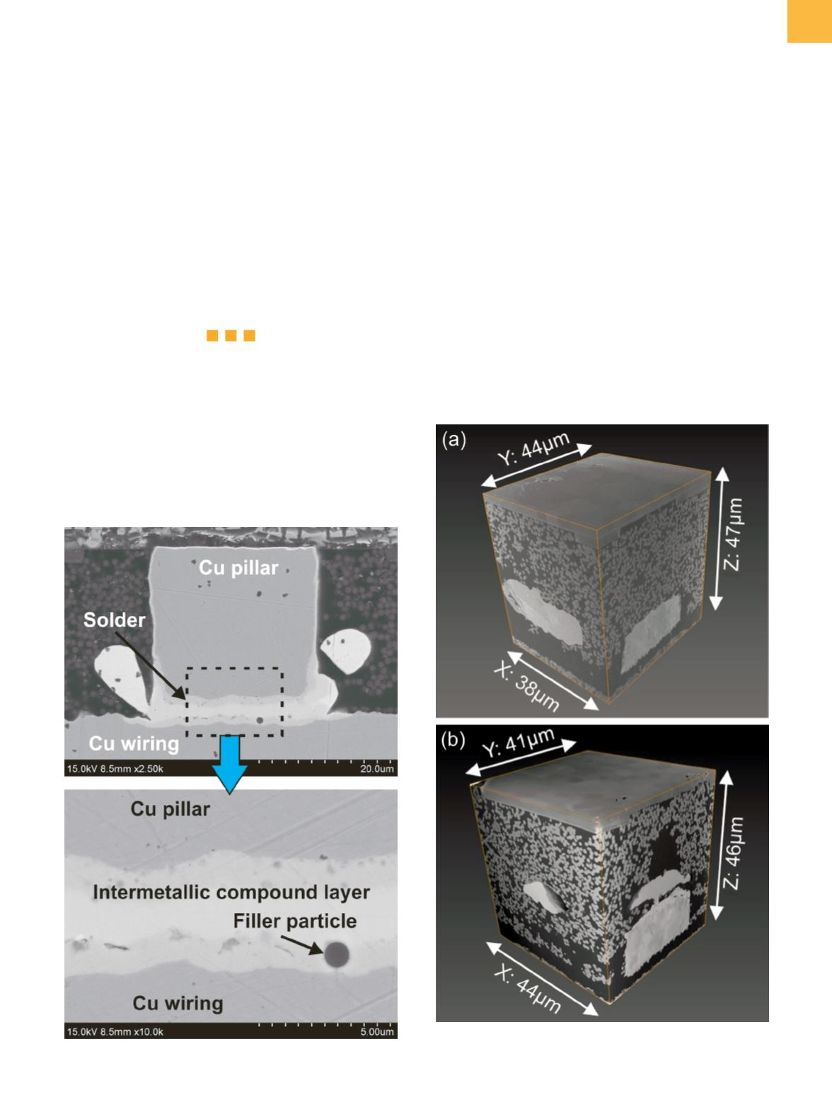
mechanical polishing is shown in Fig. 1. It seems that the
copper pillar was bonded to the copper wiring on the sub-
strate by TCB using a preapplied underfill. Figure 2 shows
higher-magnification images taken by SEM. An entrapped
filler particle from the preapplied underfill is visible in the
solder joint area.
Fig. 2
Cross-sectional SEM images of the flip-chip joint
Fig. 3
Three-dimensional reconstructed images of the flip-
chip joint. (a) Before TCT. (b) After TCT
“THE USE OF COPPER PILLAR WITH A
SOLDER CAP HAS THE ADVANTAGE OF
GANG FINE-PITCH BUMPING BY WAFER
PLATING. INCREASES IN THE NUMBER
OF BUMPS, NARROWING OF PITCH, AND
COST PRESSURES HAVE DRIVEN THE
ADOPTION OF COPPER PILLAR/SOLDER
CAP BUMPING IN HIGH-PERFORMANCE
MOBILE DEVICES. ”
3-D TOMOGRAPHIC RECONSTRUCTION
Figure 3 shows 3-D reconstructed
images
of
the
joint
before
and
after
TCT
. The volume of the reconstructed
space of the joint before TCT is
38
×
44
×
47
μm
3
, and
the volume after TCT is
44
×
41
×
46
μm
3
. Tomographic
images of the
XZ
- and
YZ
-planes of the bump center are
shown in Fig. 4.
The
XY
-plane is parallel to the substrate plane. The
X
-axis is parallel to the copper trace on the substrate, and
the
Y
-axis is perpendicular to it
. The authors observed large
voids,
shown
in Fig. 4(a) and (b) as “Voids (A).” The authors
believe these were generated by solder shrinkage.
[3]
The authors subjected another sample of the same
package to the previously mentioned TCT and then per-
formed 3-D SEM analysis of the solder joint. Another
type of void at the interface of the copper pillar and the