


 16 / 62

 edfas.org
ELECTRONIC DEVICE FAILURE ANALYSIS | VOLUME 18 NO. 1
16
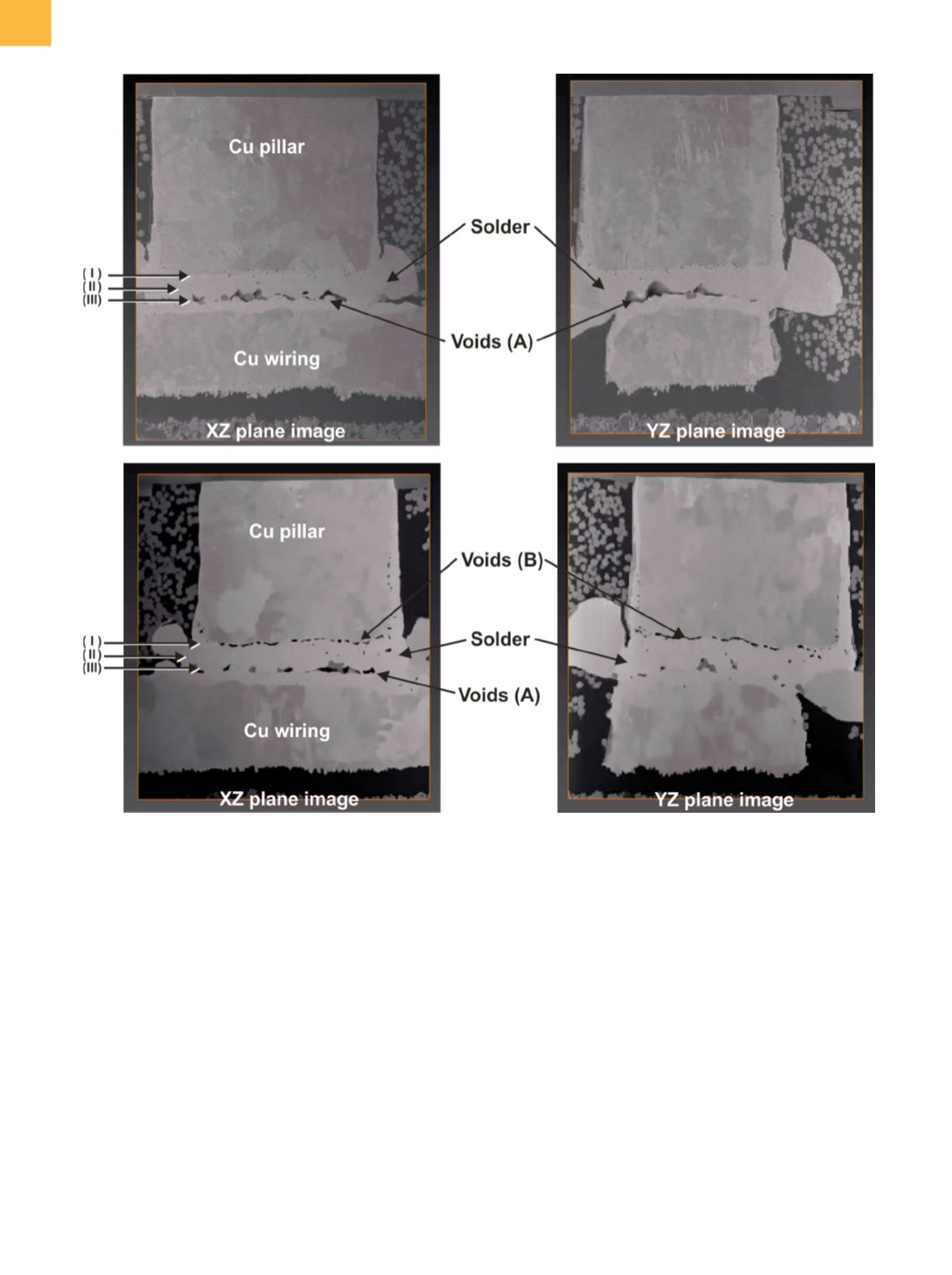
intermetallic compound (IMC) was clearly visible. These
are indicated as “Voids (B)” in Fig. 4(b).
ANALYSIS OF
XY
-PLANE SLICES
Figure 5 shows
XY
-plane t
omographic images of the
solder joints of the packages without TCT (Fig. 5a to c)
and with TCT (Fig. 5d to f). The images were extracted at
three different
Z
-heights:
• Figures 5(a) and (d), at level I (shown by arrow I in Fig.
4), are slice views of the copper pillar and IMC interface.
• Figures 5(b) and (e), at level II (shown by arrow II in Fig.
4), are slice views of the IMC layer.
• Figures 5(c) and (f), at level III (shown by arrow III in Fig.
4), are slice views at the level of the shrinkage voids.
Comparison of the two level-I views (Fig. 5a and d)
shows that the copper pillar and IMC interface changed
significantly with TCT treatment: although only small
voids are observed prior to TCT, numerous large voids
appear after TCT. At level II, v
ery
few voids
were detected
in
the
IMC
layer either before or after TCT
. At level III,
numerous shrinkage voids and entrapped filler particles
from the preapplied underfill are observed. In addition,
the authors were able to observe the 3-D
distribution
of
filler
in the underfill, as well as
gaps between the copper
pillar and the adhesive
.
(continued on page 18)
Fig. 4
Tomographic images of the
XZ
- and
YZ
-planes in the center of the copper pillar. (a) Before TCT. (b) After TCT (
–
55 °C/125 °C,
30 min/30 min, 1000 cycles)
(a)
(b)