


 18 / 62

 edfas.org
ELECTRONIC DEVICE FAILURE ANALYSIS | VOLUME 18 NO. 1
18
DISCUSSION OF VOID FORMATION
MECHANISM
The mechanism
of
void
formation
at
the
interface
between the
copper pillar and
IMC
layer
that occurs during
TCT is discussed below
.
KIRKENDALL EFFECT
The Kirkendall effect, which describes the forma-
tion of voids at the interface of different metals due
to differences in the metals’ thermal diffusivity, is well
known.
[3,4]
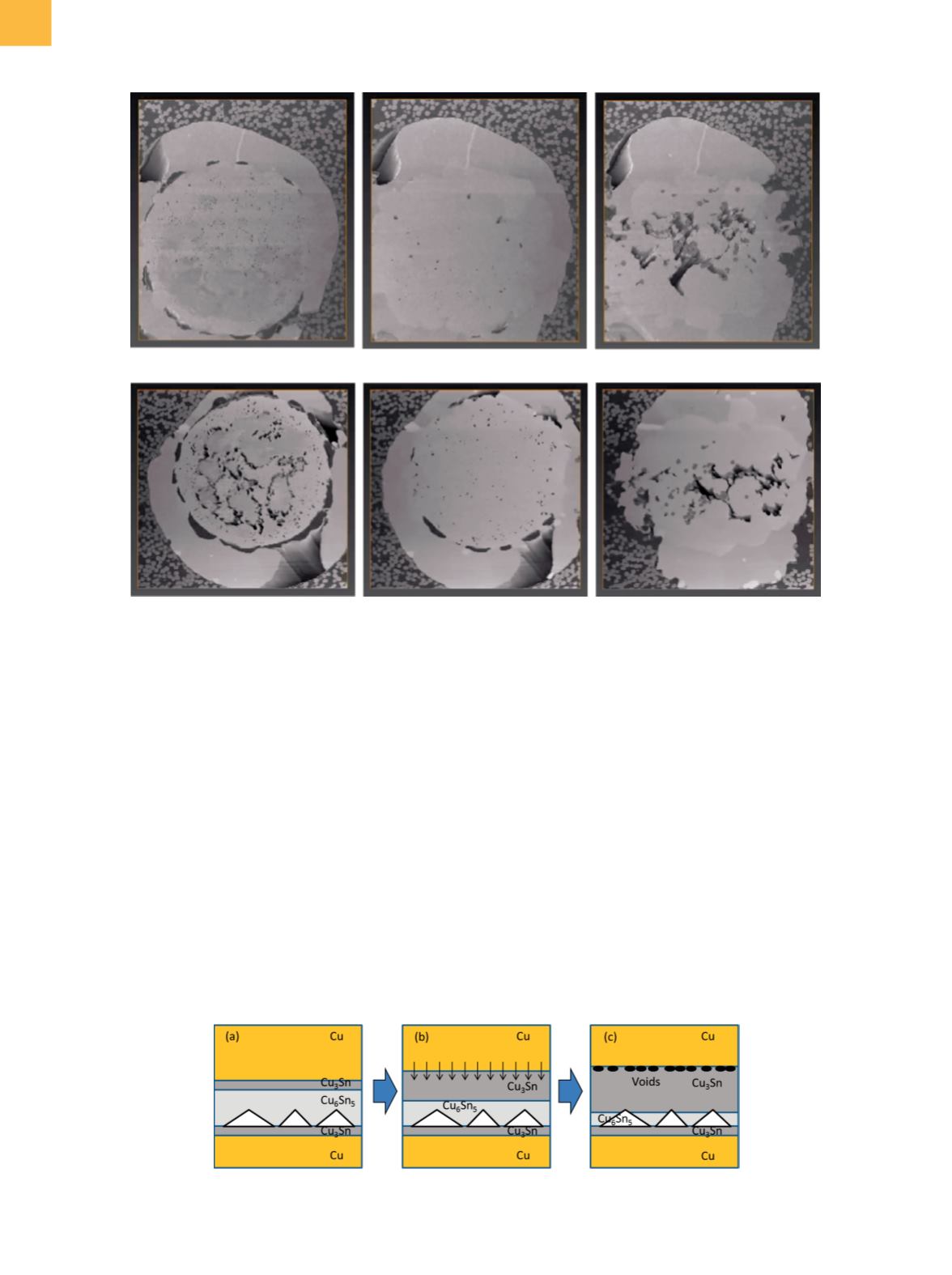
In a copper/tin system, as shown in Fig. 6,
a Cu
3
Sn IMC layer can easily grow, which creates the
Kirkendall effect. The EPMA mapping results of the IMC
layer in the authors’ system are shown in Fig. 7. Because
there is not much growth of the Cu
3
Sn layer, it does not
appear that the large-volume voids shown in Fig. 5(d) were
formed by the Kirkendall effect. This is supported by the
fact that no such voids were observed at the interface of
the substrate copper and the IMC.
GAS EXHAUST PHENOMENON AND SOLID-
PHASE DIFFUSION
Studies have shown that volatile
constituents
inside a
plated
copper
film
can move
during soldering processes,
which can lead to void
formation
in
the
solder.
[5]
3-D ANALYSIS OF A COPPER FLIP-CHIP INTERCONNECTION
(continued from page 16)
Fig. 5
Tomographic images in the
XY
-plane of the interface between copper pillar and IMC layer. (a) to (c) Before TCT.
(d) to (f) After TCT
Fig. 6
Mechanism of void formation in the system of copper diffusion model. (a) Before TCT. (b) Growth of Cu
3
Sn. (c) Kirkendall
voids formation
(a)
Slice at Interface (I)
(d)
Slice at Interface (I)
(b)
Slice at IMC layer (II)
(e)
Slice at IMC layer (II)
(c)
Slide at shrinkage void (III)
(f)
Slide at shrinkage void (III)