


 23 / 62

 edfas.org
23
ELECTRONIC DEVICE FAILURE ANALYSIS | VOLUME 18 NO. 1
important packaging requirements. The demand for thin
and stacked-dice packages that are as thin as possible led
to the development of improved bond head control algo-
rithms andmanynewloopshapeoptions.Memorydevices
often have their bond pads located down the center of
the die surface rather than around their periphery. This
allows better signal and voltage distribution and results
in faster devices that command premium values. Figure
2(a) is a photo of low loop wires for memory. These loops
rise to a low height and then travel parallel to the edge of
the die, where they descend to the second bond. Stacked-
dice packages (Fig. 2b) often employ a hybrid bond called
a stand-off stitch (SOS). In an SOS bond, a ball is formed
and bondedwith thewire intentionally broken in theHAZ.
Another ball is formed and bonded to the substrate side of
the package. The stitch (second bond) side of the wire is
thenbondedon topof the original ball. Because it requires
the formation of three bonds rather than two, the SOS
bond is approximately 40%slower than a standard bond,
but it provides the lowest loop height available. Every
smart phone (more than1billionannually) has at least one
stacked-dice package. Stacked dice, because each die can
contain a separate technology (analog, digital, memory,
radio frequency), enable integration of the entire system
within the package. Earlier attempts to integrate all of
these technologies on the same chip proved costly and
decreased reliability. Joining the technologies by stacking
themwithin the package became the dominant method.
The secondbond is formedby adifferent portionof the
capillary tip than the ball bond. Figure 3 is an illustration
of a capillary tip and the portions of the tip that produce
the ball bond, the loop, and the second bond. In forming
the second bond, the capillary face and outer radius are
pressed on the top of a round wire. The combination of
ultrasonic energy, bond force, heat, and time deform the
round wire into the fishtail shape and form the initial
intermetallic bond.
The mechanical and other materials properties of the
ball and the wire are significantly different. The second
bond is more diffusion-controlled than the ball bond.
WIRE BOND FAILURE MECHANISMS
Semiconductor packagesmust normallypass abattery
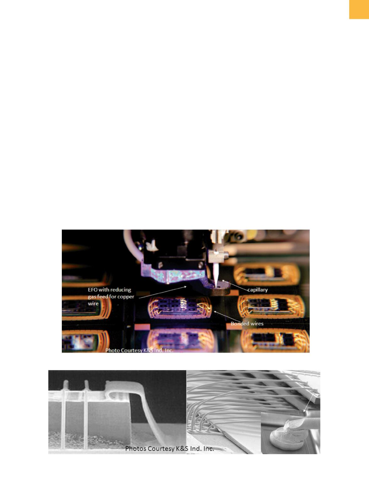
Fig. 1
Wire bonding bond head for copper wire. Courtesy of Kulicke & Soffa Industries Inc.
Fig. 2
(a) Worked loop. (b) Stand-off stitch loop. Courtesy of Kulicke & Soffa Industries Inc.
(a)
(b)