


 25 / 62

 edfas.org
25
ELECTRONIC DEVICE FAILURE ANALYSIS | VOLUME 18 NO. 1
(continued on page 28)
Instances of failures in layers below the surface, allowing
electromigration and eventually resulting in interlayer
shorts, are well documented. Often these failures can
occur while the top metal layers and wire bond are unaf-
fected.
[3]
They are difficult to detect and analyze. A team
approach, involving fab, assembly, and reliability engi-
neers, must focus on the development of pad structures
that not only can achieve electrical design requirements
but are robust enough to withstand manufacturing and
reliability.
CONCLUSION
Wire bonding continues to be the lowest-cost, highest-
reliability, most flexible semiconductor interconnection
method. It continues to reinvent itself; as new demands
are understood, machine, wire, tool, and end users come
together to find solutions that enable successful imple-
mentation of the new requirements. Each newgeneration
of devices has required increased capabilities for both
manufacturing and metrology. Wire bonding has met
these challenges and added the capabilities necessary
for its continued growth as the leading semiconductor
interconnection method.
REFERENCES
1. M. Sheaffer, L. Levine, and B. Schlain: “Optimizing the Wire Bonding
ProcessforCopperBallBondingUsingClassicExperimentalDesigns,”
Proc. Int. Electron. Manuf. Technol.
(IEMT),
Sept. 1986, pp. 103-08.
(b)
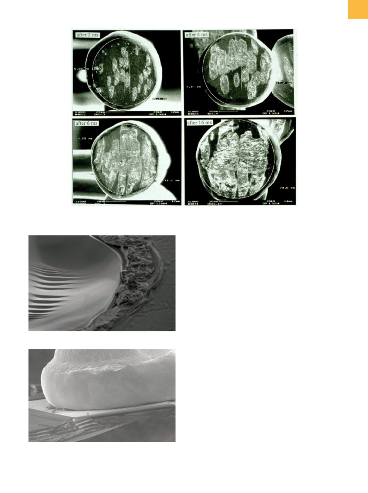
Fig. 4
Thermosonic (120 kHz) ball etch-off patterns showing weld-growth formation. Courtesy of ESEC (now BESI North America)
Fig. 5
(a) Fracture of silicon die below bond. (b) Fracture of
multilevel bond pad
(a)