


 30 / 62

 edfas.org
ELECTRONIC DEVICE FAILURE ANALYSIS | VOLUME 18 NO. 1
30
EDFAAO (2016) 1:30-35
1537-0755/$19.00 ©ASM International
®
PLASMA FIB PROVIDES VITAL DELAYERING AND SITE-
SPECIFIC FAILURE ANALYSIS CAPABILITIES FOR
LARGER-SCALE STRUCTURES
Surendra Madala, FEI
Surendra.madala@fei.comT
he plasma focused ion beam (PFIB) differs fromthe
conventional FIB in its use of a xenonplasma-based
ion source instead of the gallium liquid metal ion
source. ThePFIBcangenerate ionbeamswithmuchhigher
current and therefore is able to remove larger volumes
of material at much faster rates while still maintaining
precise control of the beam and its milling action. PFIBs
can deliver beam currents ranging from 1.5 pA to >1 µA,
with milling rates some 20 to 100 times higher than a
gallium beam due to the much higher maximum beam
current achieved by the inductively coupled plasma
source, leading to new applications in delayering/depro-
cessing and site-specific failure analysis.
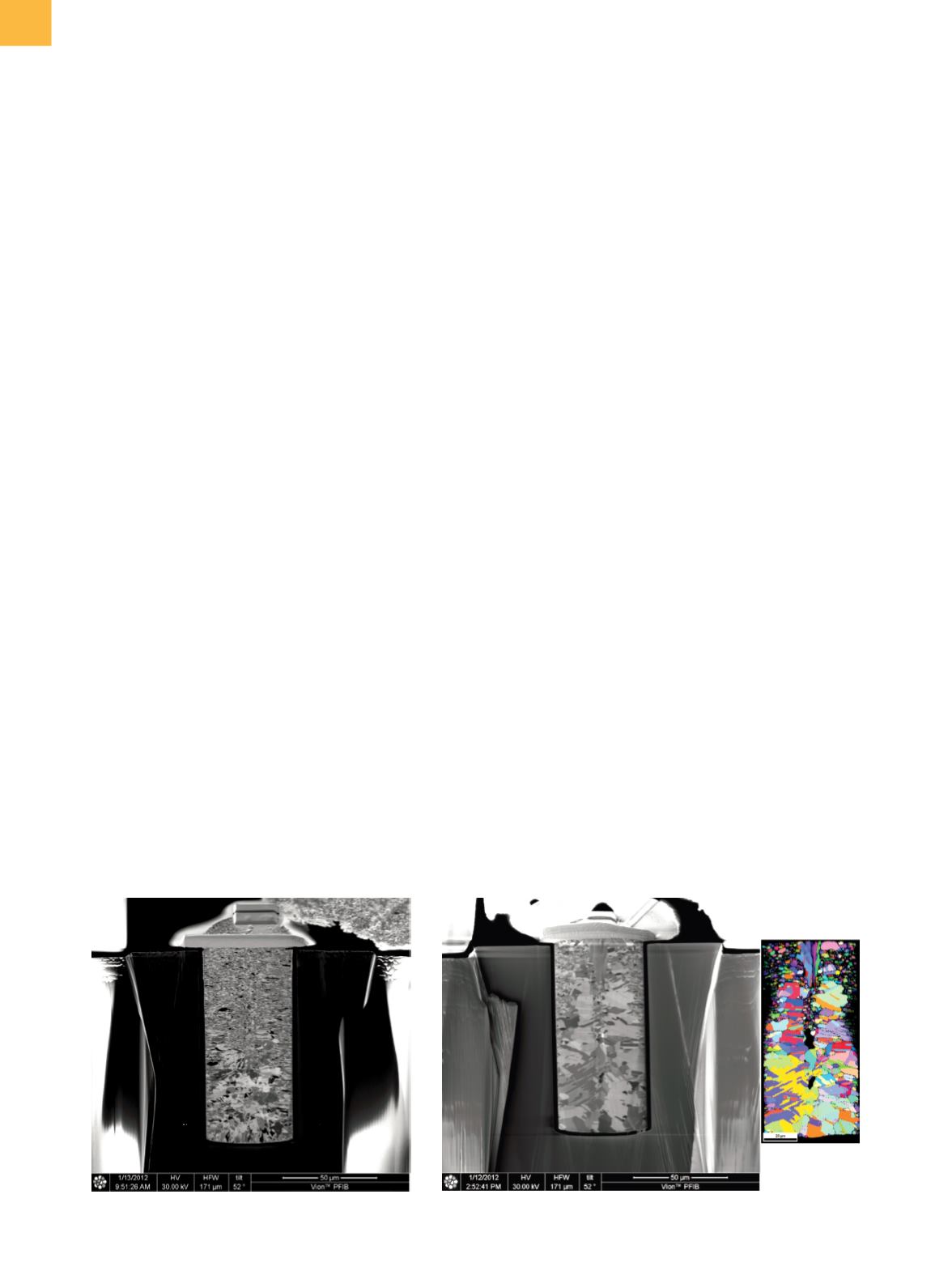
CROSS SECTIONING
COPPER-FILLED TSVs
One of the first PFIB applications was cross section-
ing copper-filled through-silicon vias (TSVs).
[1,2]
The large
dimensions of TSVs require the removal of a little more
than amillion μm
3
to create 100
×
100 μm
2
cross sections.
The PFIBmilling rates can accomplish the task in a reason-
able time. Figure 1 shows an example of a cross section
of a 50-μm-diameter
×
150-μm-deep copper-filled TSV.
PACKAGE-LEVEL CIRCUIT
MODIFICATIONS
PFIB systems have now been used successfully
to create prototypes that incorporate package-level
modifications.
[3]
Making design changes and creating
new prototypes typically takes one to two weeks. PFIB
technology can make modifications in less than a day,
significantly shortening the design and test cycle.
In some cases, packaging structures are large enough
(>100 μm) to permit modifications with laser-based
systems;
[3]
however, advanced packaging processes now
coming into production frequently use signal traces in
themiddle range (10 to 100 μm)—too big for conventional
FIB modification and too small for lasers. PFIB permits
modifications of these advancedpackage circuit elements
withinapractical time frameandwithnoneof the thermal-
or debris-associated issues of laser processing. Figure 2
shows an example of a prototype created by temporarily
relocating gold bondwires to access copper traces below.
Note the cutting of adjacent traces and rerouting of the
signal with cuts, connections, and insulation.
Fig. 1
PFIB cross section of 50-µm-diameter
×
150-µm-deep copper-filled TSV followed by electron backscatter diffraction analysis