


 32 / 62

 edfas.org
ELECTRONIC DEVICE FAILURE ANALYSIS | VOLUME 18 NO. 1
32
through-encapsulant vias, and microbumps are consid-
ered some of the most promising enabling technologies
for “More than Moore” solutions.
[5]
These technologies
involve vertical dice stacking or chip embedding with
high-density interconnects and are based on combina-
tions of process steps that come from formerly strictly
separated technology areas. Thus, there is an increasing
need to understand a large number of different interface
properties between different interconnects and, with
any encapsulation or lamination materials, to control
and optimize process steps and layer thicknesses and to
avoid any defect formation that potentially could affect
the component’s reliability. This complexity in terms of
design, new materials, and material combinations also
requires the development of newsystem-adequate failure
analysis tools capable of providing information on adhe-
sion mechanisms, interdiffusion, and phase formation
processes, or on electrical short, crack, and void forma-
tion issues. Therefore, there is a demand for metrology,
physical characterization, and failure analysis of a wide
range of 3-D interconnect technologies and relevant pro-
cesses, and also for preparation and analysis techniques
that allow access to buried structures providing physical
information at the nanometer scale within a large field
of view. Depending on the material under investigation,
both the higher current and the higher sputter efficiency
of xenon significantly improve the range of application
fields and/or the analysis throughput. Thismakes thePFIB
a very attractive tool for the analysis of relatively large
interconnect structures without any need for mechanical
preparation steps.
An open TSV interconnect technology has been devel-
oped as an alternative to copper-filled TSVs. The Bosch
etching process, combined with further IC processing
steps, is used to form TSV structures with sidewall isola-
tions and metallization with titanium/TiN, tungsten, and
aluminum. Finally, the TSVs are cappedby a silicondioxide
film and silicon nitride layers. For process optimization
and failure analysis, the sidewall layer structure must be
imaged and measured. Rapid PFIB milling can provide
precise cross sectioning to gain access to specific TSV
areas of interest or to defect siteswithin the TSV structure.
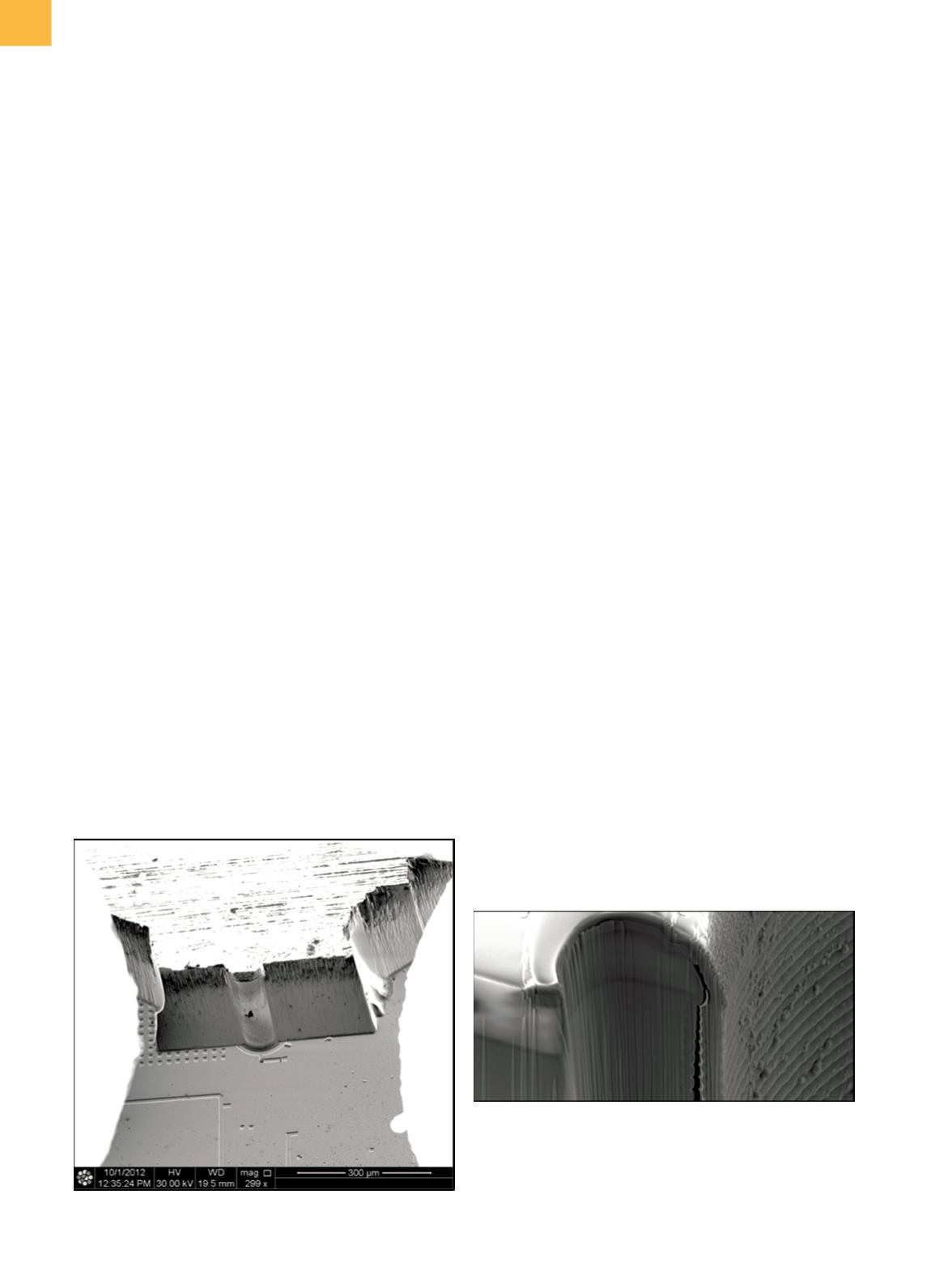
Figure 4 shows anopenTSVwith localizeddelaminated
sidewall layers. To find the root cause, the delaminated
sidewall interface shouldbeanalyzedby scanningelectron
microscope (SEM) and transmission electronmicroscope
imaging. In this case, mechanical grinding was not an
option for rough cross sectioning, because of the high risk
to fully detach the delaminated sidewall layer. Therefore,
rapid PFIB milling with a 1.3 μA xenon beam was applied
to obtain a cross section through the middle of the TSV. A
box of 700
×
300 μm and 500 μm was milled within only
5 h. Then, local sidewall polishing at 70 nA was done at
the upper left of the TSV, followed by SEM imaging of the
delaminated sidewall layer.
DIE-TO-DIE INTERCONNECTS
A fundamental requirement for any 3-D interconnect
scheme is a method for connecting the stacked dice to
each other and/or to any interposers used. Stacking
schemes may use a combination of face-to-face, face-
to-back, and die-to-interposer bonding and could also
involve a direct connection between the dice or include
a redistribution layer added to the front/back of the origi-
nally manufactured die. Whatever the scheme, there are
typically some similar challenges for creating site-specific
sections of the interconnects, in particular, locating the
Fig. 4
Delamination of sidewall in open TSV, milled with PFIB. Source: Ref 2