


 31 / 62

 edfas.org
31
ELECTRONIC DEVICE FAILURE ANALYSIS | VOLUME 18 NO. 1
DELAYERING/DEPROCESSING
Delayering of integrated circuit (IC) devices is an
important tool for semiconductor failure analysis, reverse
engineering, and circuit edit activities.
[4]
Once a defect
has been localized, it is necessary to isolate, inspect,
and perform failure analysis. One method to enable this
is to remove layer after layer until the defect is exposed.
Traditionally, thiswas performedbymechanical polishing,
followed by observation in either an optical or electron
microscope. While this method can provide reproducible
results in older process nodes over large areas (which
is important for reverse engineering), it is neither site-
specific nor planar. In addition, this method does not
have predictable end-pointing, and the functionality of
the entire chip is lost due to the destructive nature of the
polishing.
The FIB offers the means to retain chip functionality
while removing only localized regions during delayer-
ing. This is a great advantage, allowing further analysis
(voltage contrast, defect analysis, electrical probing, etc.)
or circuit edit to be performed when the layer of interest
has been reached. However, it is no easy task to delayer
modern IC devices in the FIB, due to the large number of
different layers (with vastly differingmilling rates) that are
present with varying thicknesses andmechanical proper-
ties. The divergent milling rates of the different materials
present result in nonplanar delayering, often with many
layers visible at one time.
A new beam chemistry, Dx,
[4]
has been developed to
deliver planar delayering. It can mill both dielectric and
mixed-field regions uniformly. In addition to better end
results, the process is simpler because it is continuous,
without the need to stop the milling to change gas chem-
istries when different layers are encountered. In addition,
the reduced enhancement of themilling improves control-
lability, which is an important considerationwhen dealing
with sub-100-nm-thick layers.
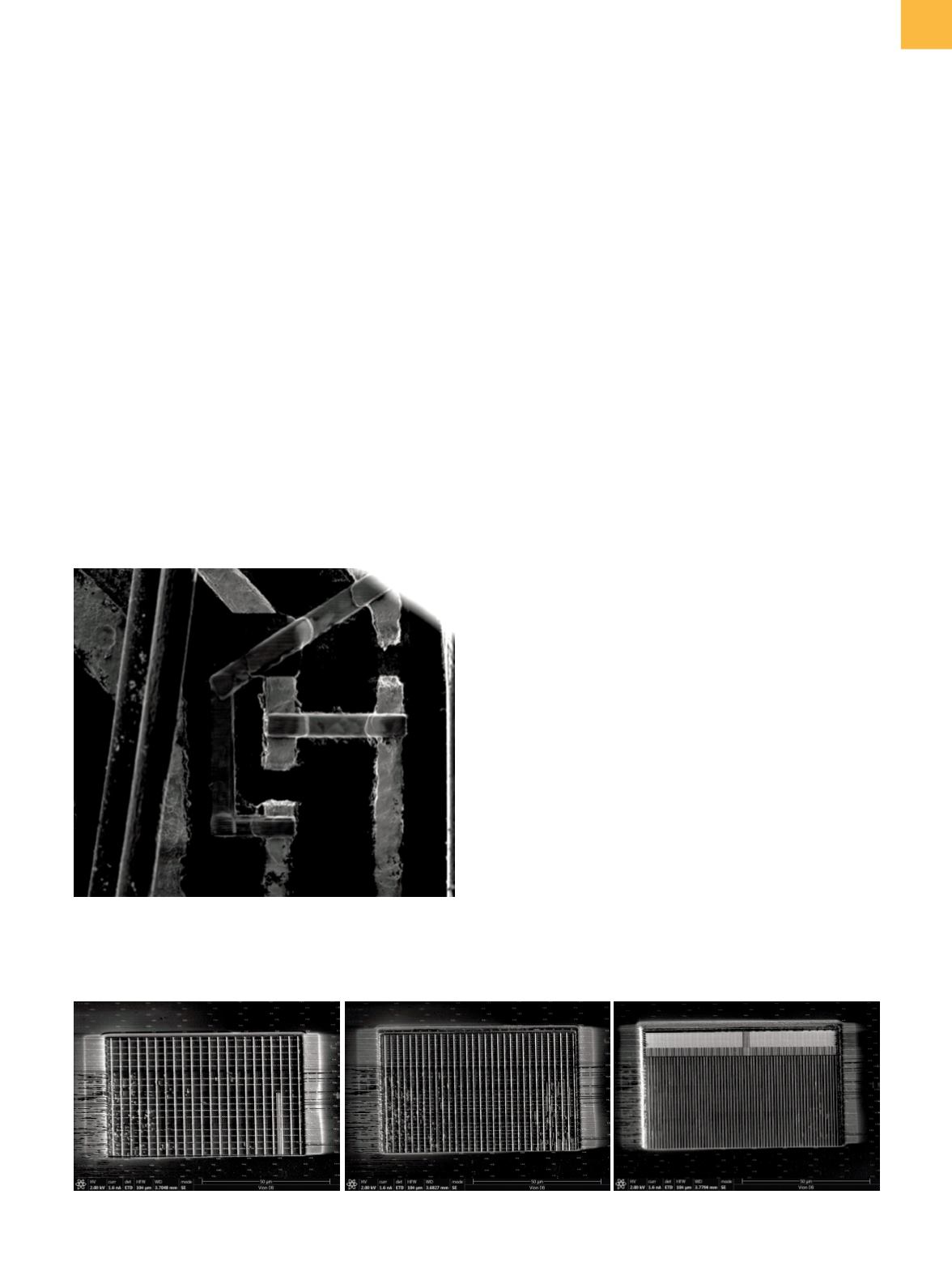
An example of the delayering possibilities when Dx
is combined with the xenon beam can be found in Fig. 3.
Here, a 22 nm device has been delayered from the front
side. The images show the excellent planarity achieved
by delayering through a stack of six copper metal layers
andSiO
2
and low-k dielectrics using the significantly larger
beam currents than are available on the gallium FIB for
delayering. Despite these larger currents, no degradation
of the planarity in the trench is observed.
The combination of delayering with Dx and the xenon
PFIB produces a more representative surface, which
is important for (in situ) nanoprobing experiments.
Implantation from the xenon ion species is lower than
gallium, but gallium, being a metal, produces some
conductive redeposit on the surface. This does not occur
when the xenon beam is used, and amore pristine surface
results. This allows proper electrical characterization to
be carried out through nanoprobing.
SITE-SPECIFIC FAILURE ANALYSIS
Today, 3-D system-in-package integration together
with advanced interconnect technologies based on TSVs,
Fig. 2
Package-level edit with xenon PFIB consisting of two
copper trace cuts and two platinumconnections while
preserving electrical functionality with insulator
deposition
Fig. 3
100
×
100 µm trench exposing (left to right) M9, M7, and M5 on a 22 nm device