


 34 / 62

 edfas.org
ELECTRONIC DEVICE FAILURE ANALYSIS | VOLUME 18 NO. 1
34
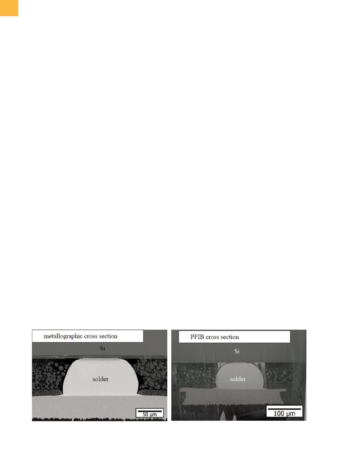
High-current PFIB milling offers a new opportunity to
cut through thewhole silicondie and solder bump contact
without any need for mechanical grinding procedures.
In this case, the solder joint contacts have a diameter
of 150 μm, which is a typical dimension. As a first step,
rapid cross sectioningwas done at the highest achievable
xenon beamcurrent of 1.3 μA. The coarse PFIBmilling of a
500-μm-long and 1-mm-deep box takes
∼
10 h of milling
time. Thefinal polishingwas doneby rockingbeammilling
at ±8° sample tilt by using a 1.3 μA xenon beam.
Figure 6 compares the PFIB-sectioned
[6]
solder joint
contact to a standard metallographic cross section.
The cross-sectional surface using PFIB preparation has
a remarkably improved quality; nearly no preparation
artifacts, for example, curtaining, are detectable. The
microstructural investigations show interface reactions
between solder joint contact and underbump metalliza-
tion. The underbump metallization shows the typical
depletion zone of the nickel-phosphorus (Ni
3
P layer) that
occurs because of the interdiffusion of nickel into the tin
solder material and the nickel-tin IMC formation at this
interface, respectively.
IN SITU ELECTRICAL FAULT ISOLATION
Transistor and interconnect-level characterization
plays a critical role during semiconductor process devel-
opment, for which samples are historically preparedusing
wet/dry etch, mechanical polishing, or conventional FIB
techniques. Using PFIB-based deprocessing techniques,
it is now possible to prepare advanced-technology-node
samples for electrical fault isolation (EFI) over large
areas (hundreds of micrometers) with higher yield and
repeatability. The EFI samples are further analyzed using
SEM image-based inspection and analysis, SEM-based
nanoprobing, or atomic force probing (AFP). Historically,
samples were polished on mechanical polishers by a
sample-preparation expert, followed by inspection on
an optical microscope or SEM to ensure that the desired
layers were reached. Then, the samples were moved to
an SEM- or AFP-based prober for further analysis by a
different set of probing experts. These two steps were
repeated for a few cycles as long as further deprocessing
was possible or until the fault was isolated. There was
a long wait time between each stage in the queue from
sample submission to final results, due to tool and opera-
tor availability, resulting in lower yields due to required
operator skills and tool capabilities.
Recent advances have enabled the integration of
sample-preparation and fault-isolation capabilities inside
a DualBeam PFIB system, thereby creating a single-tool,
single-operator solution that takes the sample from
delayering through high-resolution imaging and SEM-
based nanoprobingwithout sample transfers, wait times,
or multiple experts. This in situ preparation and analysis
approach provides faster results at a much higher yield
and in a more predictable manner. PFIB-based depro-
cessing, in combination with SEM-based imaging and
nanoprobing for localizing electrical faults, has been
performed on samples at the 10 nm node with transistor
I-V characterization, electronbeam induced current (EBIC)
on diffusion, and electron beamabsorbed current (EBAC)-
based analysis on a copper, low-k dielectric interconnect
stack. High-resolution imaging with low-beam-energy
SEM down to 350 eV combined with low-drift probes
enables easier setup resulting in analysis, as shown in
Fig. 7(a) and (b).
With material-removal rates 20 to 100 times greater
than gallium liquidmetal ion source FIB, PFIB is becoming
an essential tool for failure analysis of larger structures
created by new advanced packaging processes. Failure
analysis and fab support labs can also take advantage
of the DualBeam PFIB’s targeted chemistries for physical
Fig. 6
PFIB-sectioned solder joint compared to metallographic cross section