


 35 / 62

 edfas.org
35
ELECTRONIC DEVICE FAILURE ANALYSIS | VOLUME 18 NO. 1
failure analysis, deprocessing and device modifications,
and workflow solutions, such as EFI sample preparation,
nanoprobing, and EBIC and EBAC for fault isolation. The
DualBeamalso offers analytical capabilities, such as EBSD
and energy-dispersive x-ray for chemical, structural, and
compositional analysis.
REFERENCES
1. F. Altman et al.: “Cross Section Analysis of Cu Filled TSVs on High
Throughput Plasma-FIB Milling,”
Proc. Int. Symp. Test. Fail. Anal.
(ISTFA),
Nov. 2012.
2. L. Kwakman et al.: “Characterization and Failure Analysis of 3D
Integrated Systems Using a Novel Plasma-FIB System,”
Proc. AIP
Conf.,
2011, p. 1395.
3. M. Gonzales et al.: “Developing Functional Prototypes by Package
Modification Using Plasma FIB Technology,”
Proc. Int. Symp. Phys.
and Fail. Anal. Integr. Circuits (IPFA),
2012.
4. P. Carleson et al.: “Delayering on Advanced Process Technologies
Using PFIB,”
Proc. Int. Symp. Test. Fail. Anal. (ISTFA),
2014.
5. F. Altman and R. Young: “Site-Specific Metrology, Inspection and
Failure Analysis of Three-Dimensional Interconnects Using Focused
Ion Beam Technology,
J. Micro/Nanolith. MEMS MOEMS
, Jan.-March
2014,
13
(1), p. 011202.
6. F. Altmann, S. Klengel, J. Schischka, and M. Petzold: “Defect
Analysis Using High Throughput Plasma FIB in Packaging Reliability
Investigations,”
Proc. IEEE Electron. Compon. Technol. Conf. (ECTC),
2013.
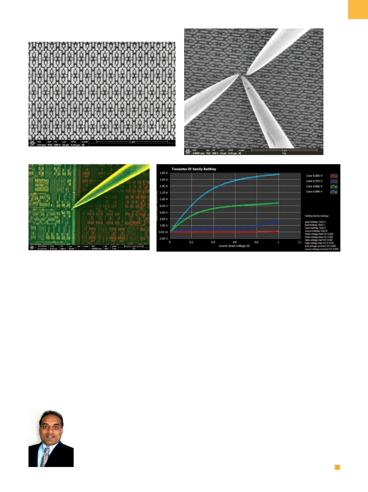
(a)
(b)
Fig. 7
(a) 22-nm-node sample deprocessed to contact level with PFIB with probe touchdown. (b) Transistor characteristics of a
22-nm-node device
ABOUT THE AUTHOR
Surendra Madala
is a product marketing manager at FEI in Hillsboro, Ore., focusing on large-area
sample preparation and advanced packaging analysis solutions. He has 20 years of experience in the
areas of IC diagnostics, circuit edit,
IC product engineering, physical and electrical failure analysis and
fault isolation, and semiconductor analytical equipment development and marketing. He holds an
MBA from Southern Methodist University, a Master’s in electrical engineering from the University of
Houston, and a Bachelor’s degree in electrical engineering fromNagarjuna University, India. Surendra
is a member of EDFAS and SEMI.