


 33 / 62

 edfas.org
33
ELECTRONIC DEVICE FAILURE ANALYSIS | VOLUME 18 NO. 1
area of interest within the stack and then gaining access
to the interface in a timely manner, often through a full
die thickness.
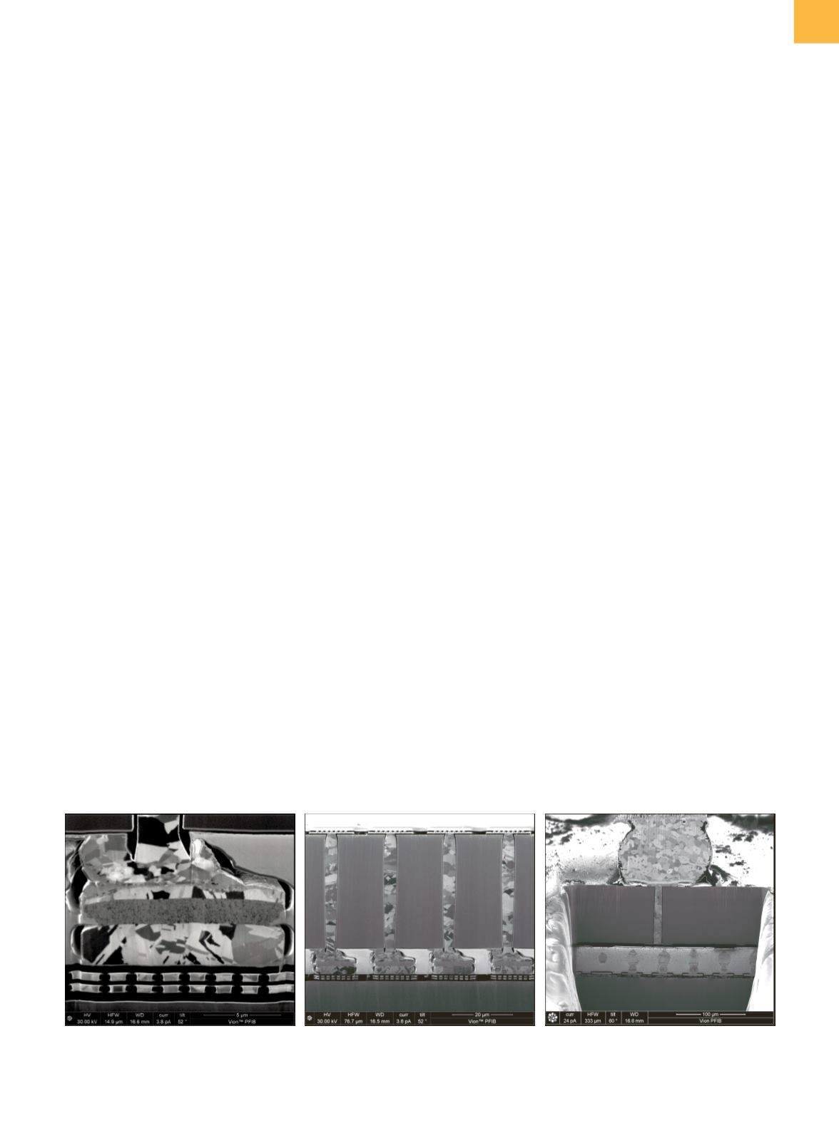
Figure 5 shows examples of three bonding schemes:
face-to-face, face-to-back, and silicon interposer. The
first example (Fig. 5a) is a face-to-face bonding layout,
where a series of Kelvin structures had been created in
a reliability test structure. In such a structure, the part of
the device stack accessible to the ion beam is the silicon
substrate of the upper die. An in situ infrared microscope
was used to image through the silicon substrate to locate
the area of interest.
After locating the area of interest, the PFIBpreparation
took 41 min to expose the section (using beam currents
from 1.3 μA to 59 nA). Like earlier figures, these images
show the utility of ion beam microscopy on the cross-
sectional face. In particular, the different components
(intermetallic compounds, or IMCs) that make up the
interconnect stack can be observed as layers of differ-
ing contrast and grain structure (e.g., large, small, or no
grains visible), which will be characteristic of each mate-
rial composition. By characterizing a comparable device
with electron backscatter diffraction
(EBSD) or similar
technique, a translation from FIB contrast and grain
structure tometallurgical composition canoftenbemade,
allowing analysis of the bonding process, including layer
thicknesses, to be obtained directly from the FIB image.
Figure 5(b) shows a face-to-back bonding scheme
incorporating TSVs. Here, a series of 31 TSVs and asso-
ciated die-to-die bonds were sectioned. The sample
preparation took
∼
2.5 h. In a subsequent step, the cross-
sectional face was milled further to expose the next set
of TSVs; this took an additional 61 min of milling. The FIB
images again show the details of the bonding process
as well as some voids in the underfill around the bonds.
Such images could also be used to assess die-to-die
alignment or make other critical measurements that can
only be assessed once the completed 3-D structure has
been assembled. In addition, the localized nature of the
sectioning means that multiple sections can be made,
even at different angles, which allows more data to be
collected from a single device.
Figure 5(c) is a failure analysis investigation on an
interconnect stack that included a packaging bump
onto a silicon interposer with a TSV, which was then
microbumped to the lower die. The sample was part of a
reliability burn-in test, and the sectioningwas targeted at
microbumps thought tobe responsible for sample failures.
The main section took <2 h. When the microbumps were
imaged with the FIB, evidence of a problem at one of the
interfaces was noted. Higher-resolution SEM imaging of
a subsequent slice through the defect showed a clear
delamination. Further delamination examples on other
microbumps were also found with the PFIB.
DIE-TO-PACKAGE INTERCONNECTS
Strength, quality, and reliability properties of inter-
connects in microelectronic packaging and microsystem
integration are closely related to the formation, growth,
and physical properties of the different IMCs formed in
the interfaces of solder joint contacts. Metallographic
grinding techniques are typically used for cross sectioning
to characterize the IMC and interfaces to the upper and
lower metallization. However, mechanical grinding could
cause artifacts such as smearing effects or crack forma-
tion caused by the mechanical impact during grinding.
Additionally, sometimes it is helpful to access selected
solder bump contacts on one device from different direc-
tions, which is not possiblewithmechanical grinding. The
PFIBpreparation provides a very precise navigation to the
region of interest by sample imaging. Cross sections can
easily be aligned in different directions.
Fig.
5
(a) Face-to-face, (b) face-to-back, and (c) silicon interposer cross sectioned by PFIB
(a)
(b)
(c)