


 19 / 62

 edfas.org
19
ELECTRONIC DEVICE FAILURE ANALYSIS | VOLUME 18 NO. 1
Void formationbasedon this gas exhaust phenomenon
is illustrated in Fig. 8.
A copper pillar
is formed bymicroplat-
ing with a certain aspect ratio, whereas
the
copper
trace
on the substrate is formed from
dense electrolytic copper
foil
. V
olatile
constituents
in
the
copper pillar
are released
as gas
during the TCT
by
interface reaction with the solder
.
SUMMARY
The authors used 3-D SEM analysis to investigate the
flip-chipbump interconnectionof anAP taken froma com-
mercial tablet PC. The analysis technology is based on the
repetition of FIB etching and SEM image capture. Three-
dimensional views were reconstructed from 240 SEM
images that were taken after repeated FIB etching at 200
nm intervals. The authors believe the interconnection to
be a copper pillar with a solder cap connected to a copper
trace on the substrate by thermal compression bonding
with a preapplied underfill. Our analysis showed that
the interconnection joint in the AP as received included
filler entrapment and many voids. With this method, the
generation of a number of voids was clearly observed at
the interface of the pillar copper and the IMC after 1000
cycles of TCT between
-
55 and 125 °C.
REFERENCES
1. M. Lee et al.: “Study of Interconnection Process for
Fine Pitch Flip Chip,”
Proc. 59th Electron. Compon.
Technol. Conf. (ECTC),
2009, pp. 720-23.
2. M. Ritter and P.A. Midgley: “A Practical Approach to
Test the Scope of FIB-SEM3DReconstruction,”
J. Phys.
Conf. Ser.,
2010,
241,
p. 012081.
3. Y. Orii et al.: “Micro Structure Observation and
Reliability Behavior of Peripheral Flip Chip Inter
connections with Solder-Capped Cu Pillar Bumps,”
Trans. Jpn. Inst. Electron. Packag.,
2011,
4
(1), pp. 73-86.
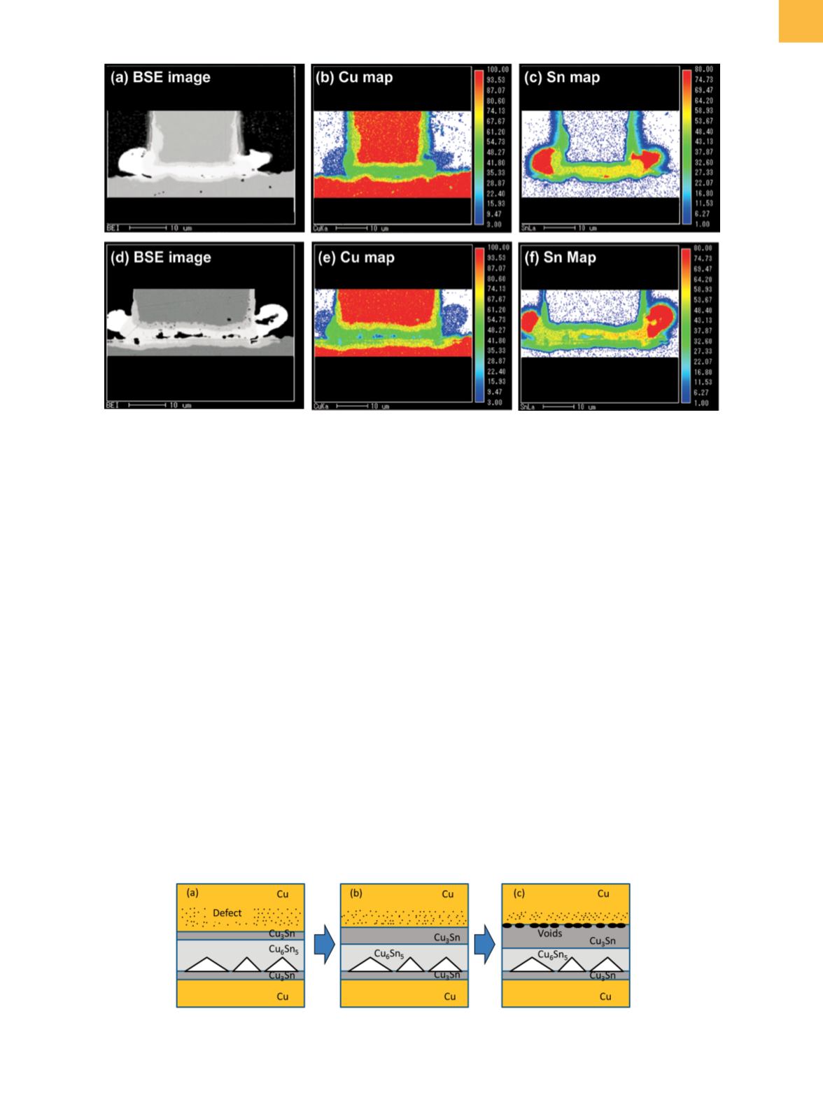
Fig. 7
EPMA mapping of solder joint on flip-chip. (a) to (c) Before TCT. (d) to (f) After TCT. BSE, backscattered electron
Fig. 8
Mechanism of void formation in the system of gas exhaust model in solid-phase diffusion. (a) Before TCT. (b) Slight growth
in Cu
3
Sn. (c) Void formation by accumulation of defects