


 14 / 62

 edfas.org
ELECTRONIC DEVICE FAILURE ANALYSIS | VOLUME 18 NO. 1
14
3-D ANALYSIS OF A COPPER FLIP-CHIP
INTERCONNECTION USING FIB-SEM SLICE AND VIEW
Mototaka Ito and Jun Kato, Toray Research Center
Mototaka_Ito@trc.toray.co.jpR
ecently, flip-chip
assembly has become
mainstream
for fine-pitch
interconnection
in large-scale integra-
tion packages. Gold
studs and copper
pillar
s with
solder caps
are two types of bumps in common use.
[1]
Gold
stud bumps are commonly used
for interconnecting dice
withperipheral layouts. Gold-goldbonding has the advan-
tage of a low process temperature, and gold-solder with
adhesive has good wettability of the joint without flux.
The use of copper
pillar
with a solder cap has the
advantage of gang fine-pitch bumping by wafer plating.
Increases in the number of bumps, narrowing of pitch, and
cost pressures have driven the adoption of copper pillar/
solder cap bumping in high-performancemobile devices.
Copper pillar bumps on the die are interconnected to the
copper padon the substrate ina solder reflowprocess. The
useof thermal compressionbonding (TCB) andpreapplied
underfill for fine-pitch interconnection is growing due to
its precise alignment of bump and pad and theminimiza-
tion of global stress on the assembly. Concerns with the
technology, however, include entrapment of adhesive
components and voids in the joint due to solder shrinkage.
FIB-SEM FOR FLIP-CHIP JOINT
ANALYSIS
Three-dimensional (3-D) analysis techniques can be
used to study copper pillar bump joints.
X-ray computed
tomography (
CT)
is one major 3-D analytical method, but
its
spatial resolution
is
currently limited to the submicron
level
. The slice-and-viewmethod using a focused ion beam-
secondary electron microscope (FIB-SEM) has high spatial
resolution on a nanometer level, whichmakes it superior to
x-ray CT.
[2]
This method has already been used to investigate
the inner wiring of a semiconductor device. The authors
used the method to evaluate the solder joint and what
appeared to be preapplied underfill between a copper pillar
bump and a copper trace on a substrate.
The authors removed a memory and application
processor (AP) packaged in a package-on-package (PoP)
from a commercial tablet personal computer (PC). First,
mechanical polishing was used to expose the structure
of the PoP, and then the microbump interconnecting the
AP to the copper wiring on the package substrate was
located. The authors then made a
3-D observation
by
the
slice-and-view method using
an FIB-
SEM equipped with a
dual-
electron
beam
. An
SEM
image was taken every
200 nm
of etching by FIB, for a total of 240
SEM
images
. Then, 3-D
images were
re
constructed using these SEM still images.
The authors also investigated the
composition distri-
bution
of
the
solder
joint area by
electron probe x-ray
microanalysis
(EPMA)
. To observe thermal changes in
the bumps, another sample of the PoP was subjected
to a thermal cycle test (TCT) of 1000 cycles from
-
55 to
125
°
C with a 1 h cycle.
COPPER PILLAR JOINT ANALYSIS
RESULTS
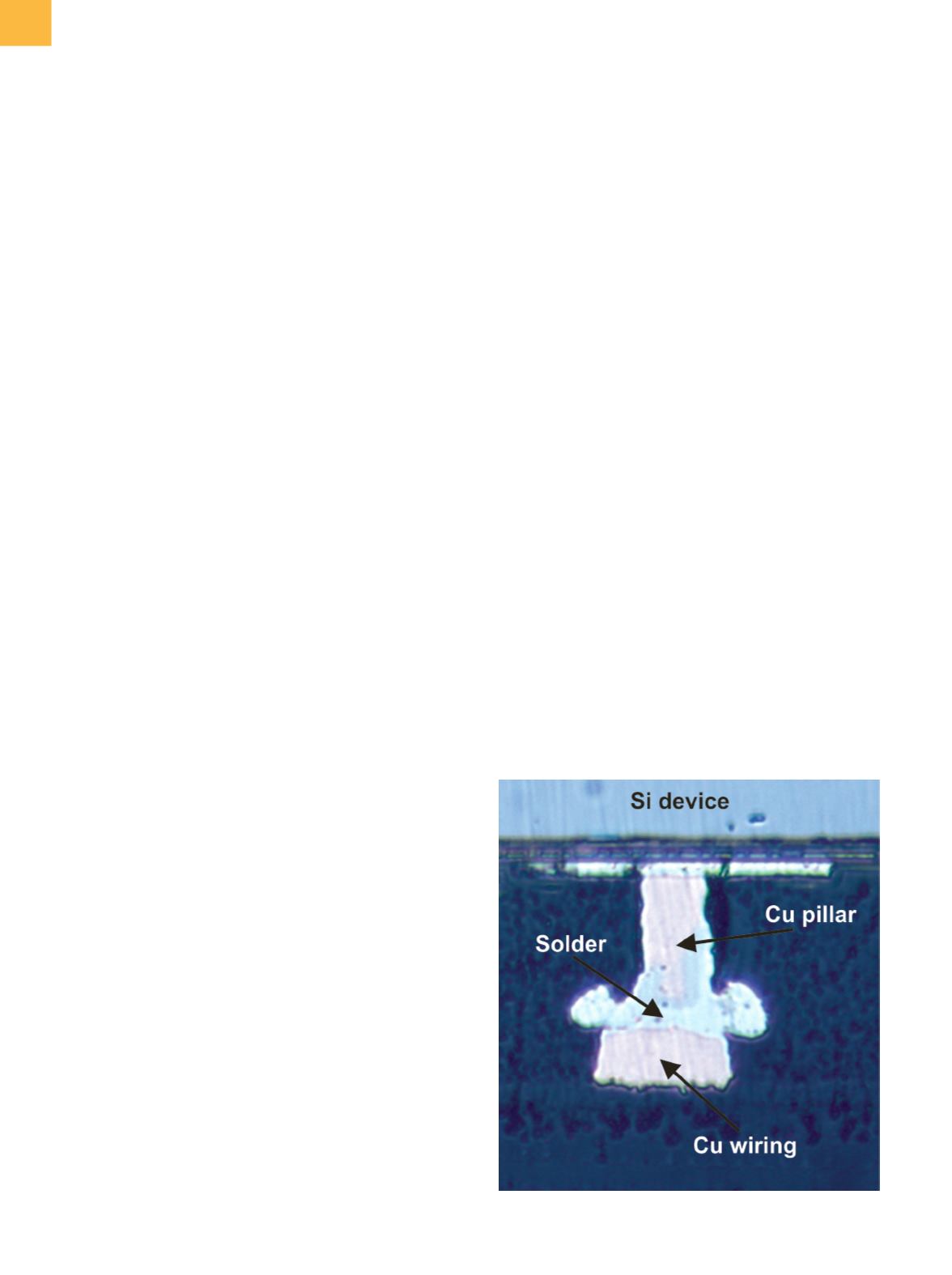
A cross-sectional microscopic image of the flip-
chip bump interconnection of the AP die prepared by
EDFAAO (2016) 1:14-20
1537-0755/$19.00 ©ASM International
®
Fig. 1
Cross-sectional micrograph of the flip-chip joint