


 11 / 62

 edfas.org
1 1
ELECTRONIC DEVICE FAILURE ANALYSIS | VOLUME 18 NO. 1
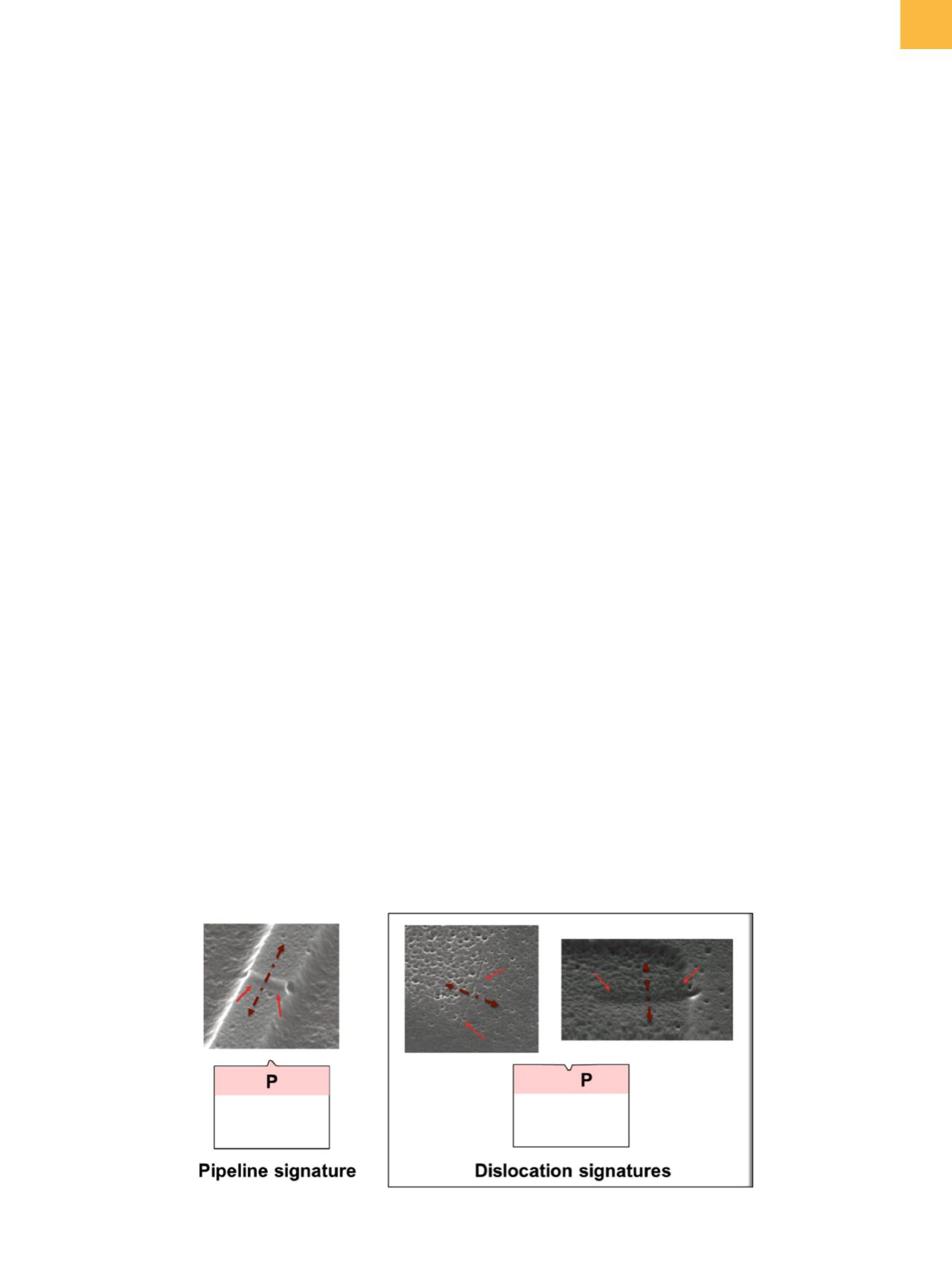
Fig. 11
Schematic cross-sectional views of silicon pipeline defect in relief compared to dislocation in silicon
(knowing that it can destroy the defect) at the silicon
level. Then, planar TEM can finalize the study of a dif-
ferent part to confirm the nature of the silicon defect.
• When only one part is available:
The FA strategy should
be different. The analysis can start by SEM PVC at the
silicon level to make a first distinction; it should be
positive in the pipeline case. Then, AFM-based dopant
profiling techniques should be employed to detect
surface-level anomalies. Depending on the sample
state after SMM, planar TEM can be used to localize
and image the defect.
HYPOTHESIS OF PIPELINE VERSUS
DISLOCATION FORMATION
As demonstrated, pipeline silicondefects are observed
inNMOS transistors and are generatedby the formation of
“diffusion pipes” at an active area channel surface under
certain process conditions, causing leakages between
implanted drain and source regions. The origin of the
defect formation is not completely understood. Based
on the literature,
[11]
reported hypotheses concerning the
formation of pipeline defects include potential stress
generated during sidewall mask isolation etch at island
corners, implant-induced silicon damage, possible physi-
cal correlation between a type of etch pit pairs, and some
design/mechanical considerations on isolation trench
walls. Despite these different aspects, it is well known
that the main solution for improving yield is to use suit-
able furnace recrystallization steps to eliminate this type
of defect.
A hypothesis is proposed that defines a link between
dislocation andpipeline defects. It is possible that disloca-
tions are the first step in the silicon substrate defect, which
can evolve into a pipeline defect under various particular
process conditions, depending on wafer fab processing,
deep-trench pattern design, process aspect (annealing,
implantation, surface oxidation), and so on.
[12]
In other
words, pipeline defects can either be the same type of
dislocations formed on the surface, or they can be formed
through dislocations pinning at the surface region.
CONCLUSIONS
Depending on the choice of FA techniques, the distinc-
tion between a dislocation and a pipeline defect in NMOS
transistors can be very difficult. Electrical investigations
through fault localization techniques are useful in deter-
mining the impacted device and its localization. Atomic
force probing enables further localization of the defective
device. However, no distinction between a pipeline and
a dislocation was observed during the electrical charac-
terizations. Nevertheless, physical investigations with a
combination of SEM PVC at the silicon level, Wright etch
delineation, nondestructive dopant profiling techniques,
and TEM techniques could be used to distinguish a pipe-
line defect froma dislocation. Proper classification, based
on interpretation of the physical signature observed
through the various methods, will determine the appro-
priate corrective actions inwafer fabmanufacturing, thus
allowing continuous improvement.
ACKNOWLEDGMENT
The author would like to thank his co-workers who
participated in the initial version of the article presented
at ISTFA 2014.
REFERENCES
1. P.M. Fahey, S.R. Mader, S.R. Stiffler, R.L. Mohler, J.D. Mis, and J.A.
Slinklman: “Stress-Induced Dislocations in Silicon Integrated
Circuits,”
IBM J. Res. Develop.,
March 1992,
36
(2), pp.158-82.
2. S.-H. Soh, J. Lari, S. Hunt, T. Davies, M. Kuo, U.S. Kim, M. Cheung, and
E. Lucero: “Relation between Etch Pit Pairs and Pipeline Defects in
CMOS Device,”
IEEE Int. Reliab. Phys. Symp. (IRPS),
1995, p. 244-48.
3. H. Belgal, G. Yuen, J. Grohs, L. Rozler, H. Gee, and S. Broydo: “A New
Mechanismof Pipeline Defect Formation in CMOS Devices,”
IEEE Int.
Reliab. Phys. Symp. (IRPS),
1994, p. 399.